|
|
|
PDF L9950TR Data sheet ( Hoja de datos )
| Número de pieza | L9950TR | |
| Descripción | DOOR ACTUATOR DRIVER | |
| Fabricantes | STMicroelectronics | |
| Logotipo | ||
Hay una vista previa y un enlace de descarga de L9950TR (archivo pdf) en la parte inferior de esta página. Total 23 Páginas | ||
|
No Preview Available !
L9950
DOOR ACTUATOR DRIVER
1 FEATURES
■ One full bridge for 6A load (ron = 150mΩ )
■ Two half bridges for 3A load (ron = 300mΩ )
■ Two half bridges for 1.5A load (ron = 800mΩ )
■ One highside driver for 6A load (ron = 100mΩ )
■ Four highside drivers for 1.5A load (ron = 800 mΩ )
■ Programmable Softstart function to drive loads
with higher inrush currents (i.e. current
>6A,>3A,>1.5A)
■ Very low current consumption in standby mode
IS < 6µA, typ. Tj ≤ 85 °C)
■ All outputs short circuit protected
■ Current monitor output for 300mΩ ,150mΩ and
100m highside drivers
■ All outputs over temperature protected
■ Open load diagnostic for all outputs
■ Overload diagnostic for all outputs
■ Seperated half bridges for door lock motor
■ PWM control of all outputs
■ Charge Pump output for reverse polarity
protection
2 APPLICATIONS
Door Actuator Driver with bridges for door lock and
safe lock, mirror axis control, mirror fold and highside
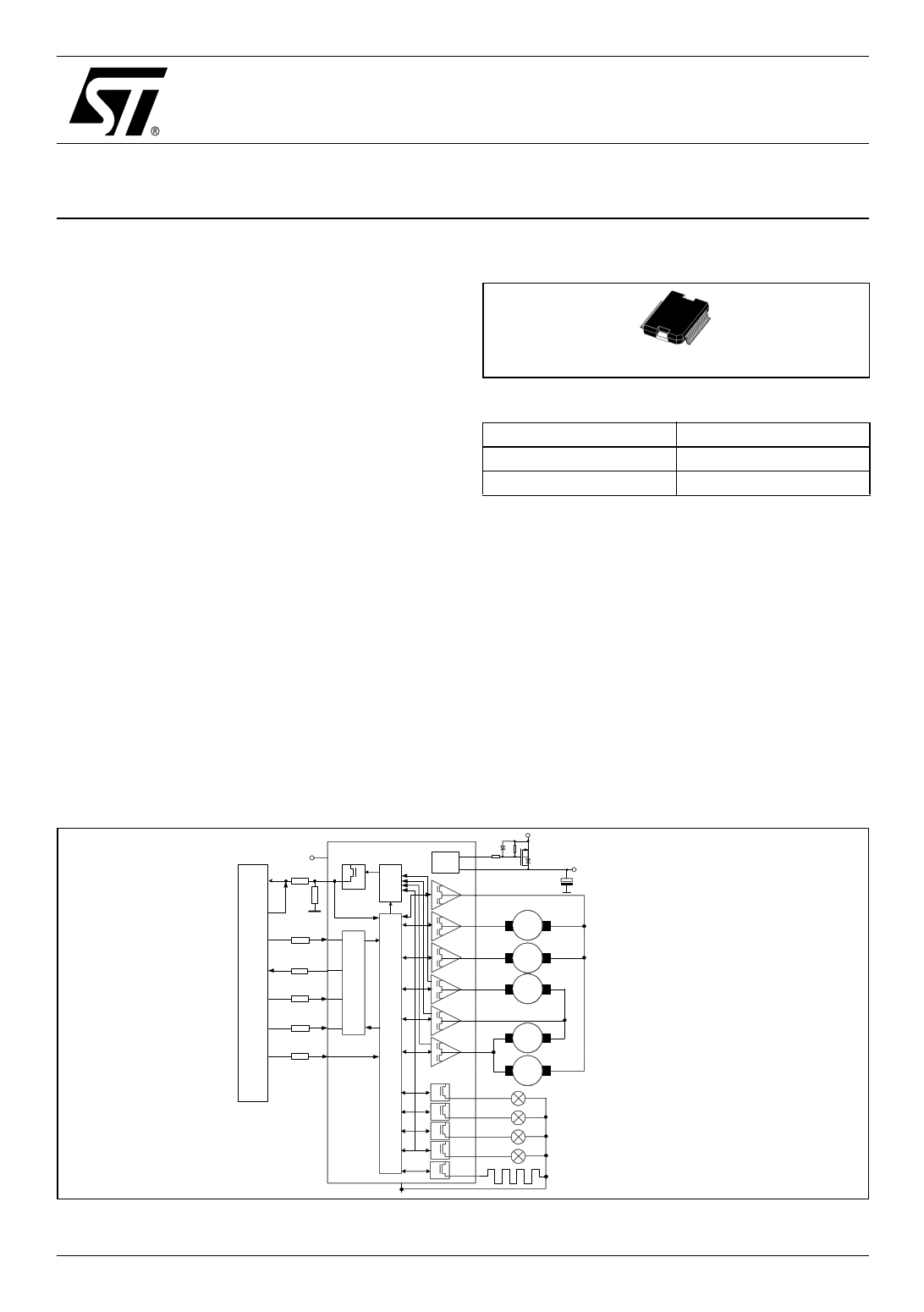
Figure 2. Block Diagram
VCC
CM/PWM2
1k
CP
PWM2
DI
1k
DO
1k
CLK
1k
CSN
1k
PW M1
1k
Note: resistors between µC and
L9950 are recommended to limit
currents for negative voltage
transients at VBAT (e.g. ISO
type 1 pulse).
GND
Figure 1. Package
PowerSO36
Table 1. Order Codes
Part Number
L9950
L9950TR
Package
PowerSO36
Tape & Reel
driver for mirror defroster and four 5W-light bulbs.
3 DESCRIPTION
The L9950 is a microcontroller driven multifunc-
tional door actuator driver for automotive applica-
tions.Up to five DC motors and five grounded
resistive loads can be driven with six half bridges
and five highside drivers. The integrated standard
serial peripheral interface (SPI) controls all opera-
tion modes (forward, reverse, brake and high im-
pedance).
All diagnostic informations are available via SPI.
VBAT
Reve rse
Polarity
10k Protection
OUT1 xy-Mirror
Motors
MOUT2
Note: value of capacitor has to be
choosen carefully to limit the VS
VS voltage below absolute maximum
ratings in case of an unexpected
freewheeling condition (e.g. TSD,
POR)
MOUT3
MOUT4
OUT5 Lock
MOUT6
Safe Lock
OUT7
OUT8
M
Mirror Fold
Exteriour Light
Footstep Light
OUT9
Safety Light
OUT10
OUT11
Turn Indicator
Defroster
July 2004
REV. 3
1/23
1 page 
L9950
Table 2. Pin Description
Pin
1, 18, 19,
36
2.35
3
4
5
6, 7, 14, 15,
23, 24, 25,
28, 29, 32
8
9
10
11
12
13
16,17,
20,21,
22
26
27
30
31
33
34
Symbol
GND
OUT11
OUT1
OUT2
OUT3
VS
DI
CM/PWM2
CSN
DO
VCC
CLK
OUT4
OUT5
OUT6
CP
PWM1
OUT7,
OUT8,
OUT9,
OUT10
Function
Ground:
Reference potential
Important: For the capability of driving the full current at the outputs all pins of GND must
be externally connected !
Highside-driver-output 11:
The output is built by a highside switch and is intended for resistive loads, hence the
internal reverse diode from GND to the output is missing. For ESD reason a diode to GND
is present but the energy which can be dissipated is limited. The highside driver is a power
DMOS transistor with an internal parasitic reverse diode from the output to VS (bulk-drain-
diode). The output is over-current and open load protected.
Important: For the capability of driving the full current at the outputs both pins of OUT11
must be externally connected !
Halfbridge-output 1,2,3:
The output is built by a highside and a lowside switch, which are internally connected. The
output stage of both switches is a power DMOS transistor. Each driver has an internal
parasitic reverse diode (bulk-drain-diode: highside driver from output to VS, lowside driver
from GND to output). This output is over-current and open load protected.
Power supply voltage (external reverse protection required):
For this input a ceramic capacitor as close as possible to GND is recommended.
Important: For the capability of driving the full current at the outputs all pins of VS must be
externally connected !
Serial data input:
The input requires CMOS logic levels and receives serial data from the microcontroller.
The data is an 24bit control word and the least significant bit (LSB, bit 0) is transferred
first.
Current monitor output/PWM2 input:
Depending on the selected multiplexer bits of Input Data Register this output sources an
image of the instant current through the corresponding highside driver with a ratio of 1/
10.000. This pin is bidirectional. The microcontroller can overdrive the current monitor
signal to provide a second PWM input for the outputs OUT9 and OUT10.
Chip Select Not input / Testmode :
This input is low active and requires CMOS logic levels. The serial data transfer between
L9950 and micro controller is enabled by pulling the input CSN to low level. If an input
voltage of more than 7.5V is applied to CSN pin the L9950 will be switched into a test
mode.
Serial data output:
The diagnosis data is available via the SPI and this tristate-output. The output will remain
in tristate, if the chip is not selected by the input CSN (CSN = high)
Logic supply voltage:
For this input a ceramic capacitor as close as possible to GND is recommended.
Serial clock input:
This input controls the internal shift register of the SPI and requires CMOS logic levels.
→Halfbridge-output 4,5,6: see OUT1 (pin 3).
Important: For the capability of driving the full current at the outputs both pins of OUT4
(OUT5, respectively) must be externally connected !
Charge Pump Output:
This output is provided to drive the gate of an external n-channel power MOS used for
reverse polarity protection (see FIGURE 1)
PWM1 input:
This input signal can be used to control the drivers OUT1-OUT8 and OUT11 by an
external PWM signal.
Highside-driver-output 7,8,9,10:
The output is built by a highside switch and is intended for resistive loads, hence the
internal reverse diode from GND to the output is missing. For ESD reason a diode to GND
is present but the energy which can be dissipated is limited. The highside driver is a power
DMOS transistor with an internal parasitic reverse diode from the output to VS (bulk-drain-
diode). The output is over-current and open load protected.
5/23
5 Page 
L9950
4.3 Serial Data In (DI)
The input pin is used to transfer data serial into the device. The data applied to the DI will be sampled at
the rising edge of the CLK signal and shifted into an internal 24 bit shift register. At the rising edge of the
CSN signal the contents of the shift register will be transferred to Data Input Register. The writing to the
selected Data Input Register is only enabled if exactly 24 bits are transmitted within one communication
frame (i.e. CSN low). If more or less clock pulses are counted within one frame the complete frame will be
ignored. This safety function is implemented to avoid an activation of the output stages by a wrong com-
munication frame.
Note: Due to this safety functionality a daisy chaining of SPI is not possible. Instead, a parallel operation of the SPI bus by controlling
the CSN signal of the connected ICs is recommended.
4.4 Serial Data Out (DO)
The data output driver is activated by a logical low level at the CSN input and will go from high impedance
to a low or high level depending on the status bit 0 (fault condition). The first rising edge of the CLK input
after a high to low transition of the CSN pin will transfer the content of the selected status register into the
data out shift register. Each subsequent falling edge of the CLK will shift the next bit out.
4.5 Serial Clock (CLK)
The CLK input is used to synchronize the input and output serial bit streams. The data input (DI) is sam-
pled at the rising edge of the CLK and the data output (DO) will change with the falling edge of the CLK
signal.
4.6 Input Data Register
The device has two input registers. The first bit (bit 0) at the DI-input is used to select one of the two Input
Registers. All bits are first shifted into an input shift register. After the rising edge of CSN the contents of
the input shift register will be written to the selected Input Data Register only if a frame of exact 24 data
bits are detected. Depending on bit 0 the contents of the selected status register will be transferred to DO
during the current communication frame. Bit 1-17 controls the behaviour of the corresponding driver.
If bit 23 is zero, the device will go into the standby-mode. The bits 18 and 19 are used to control the current
monitor multiplexer. Bit 22 is used to reset all status bits in both status registers. The bits in the status
registers will be cleared after the current communication frame (rising edge of CSN).
4.7 Status Register
This devices uses two status registers to store and to monitor the state of the device. Bit 0 is used as a
fault bit and is a logical-NOR combination of bits 1-22 in both status registers. The state of this bit can be
polled by the microcontroller without the need of a full SPI-communication cycle (see FIGURE 11). If one
of the over-current bits is set, the corresponding driver will be disabled. If the over-current recovery bit of
the output is not set the microcontroller has to clear the over-current bit to enable the driver. If the thermal
shutdown bit is set, all drivers will go into a high impedance state. Again the microcontroller has to clear
the bit to enable the drivers.
4.8 Test Mode
The Test Mode can be entered by rising the CSN input to a voltage higher than 7.0V. In the test mode the
inputs CLK, DI, PWM1/2 and the internal 2MHz CLK can be multiplexed to data output DO for testing pur-
pose. Furthermore the over-current thresholds are reduced by a factor of 4 to allow EWS testing at lower
current. For EWS testing a special test pad is available to measure the internal bandgap voltage, the TW
and TSD thresholds.
The internal logic prevents that the Hi-Side and Lo-Side driver of the same half-bridge can be switched-
on at the same time. In the testmode this combination is used to multiplex the desired signals according
to following table 8:
11/23
11 Page | ||
| Páginas | Total 23 Páginas | |
| PDF Descargar | [ Datasheet L9950TR.PDF ] | |
Hoja de datos destacado
| Número de pieza | Descripción | Fabricantes |
| L9950TR | DOOR ACTUATOR DRIVER | STMicroelectronics |
| Número de pieza | Descripción | Fabricantes |
| SLA6805M | High Voltage 3 phase Motor Driver IC. |
Sanken |
| SDC1742 | 12- and 14-Bit Hybrid Synchro / Resolver-to-Digital Converters. |
Analog Devices |
|
DataSheet.es es una pagina web que funciona como un repositorio de manuales o hoja de datos de muchos de los productos más populares, |
| DataSheet.es | 2020 | Privacy Policy | Contacto | Buscar |