|
|
|
PDF LTC6085 Data sheet ( Hoja de datos )
| Número de pieza | LTC6085 | |
| Descripción | CMOS Amplifiers | |
| Fabricantes | Linear | |
| Logotipo | ||
Hay una vista previa y un enlace de descarga de LTC6085 (archivo pdf) en la parte inferior de esta página. Total 16 Páginas | ||
|
No Preview Available !
FEATURES
n Low Offset Voltage: 750μV Maximum
n Low Offset Drift: 5μV/°C Maximum
n Low Input Bias Current:
1pA (Typical at 25°C)
40pA (≤85°C)
n Rail-to-Rail Inputs and Outputs
n 2.5V to 5.5V Operation Voltage
n Gain Bandwidth Product: 1.5MHz
n CMRR: 70dB Minimum
n PSRR: 94dB Minimum
n Supply Current: 110μA per Amplifier
n Shutdown Current: 1.1μA per Amplifier
n Available in 8-Lead MSOP and 10-Lead DFN
Packages (LTC6084) and 16-Lead SSOP and DFN
Packages (LTC6085)
APPLICATIONS
n Portable Test Equipment
n Medical Equipment
n Consumer Electronics
n Data Acquisition
LTC6084/LTC6085
Dual/Quad 1.5MHz,
Rail-to-Rail, CMOS
Amplifiers
DESCRIPTION
The LTC®6084/LTC6085 are dual/quad, low cost, low offset,
rail-to-rail input/output, unity-gain stable CMOS operational
amplifiers that feature 1pA of input bias current.
A 1.5MHz gain bandwidth, and 0.5V/μs slew rate, along
with the wide supply range and a low 0.75mV offset, make
the LTC6084/LTC6085 useful in an extensive variety of ap-
plications from data acquisition to medical equipment and
consumer electronics. The 110μA supply current and the
shutdown mode are ideal for signal processing applications
which demand performance with minimal power.
The LTC6084/LTC6085 have an output stage which swings
within 5mV of either supply rail to maximize signal dynamic
range in low supply applications. The input common
mode range includes the entire supply voltage. These op
amps are specified on power supply voltages of 2.5V and
5V from –40°C to 125°C. The dual amplifier LTC6084 is
available in 8-lead MSOP and 10-lead DFN packages. The
quad amplifier LTC6085 is available in 16-lead SSOP and
DFN packages.
L, LT, LTC and LTM are registered trademarks of Linear Technology Corporation.
All other trademarks are the property of their respective owners.
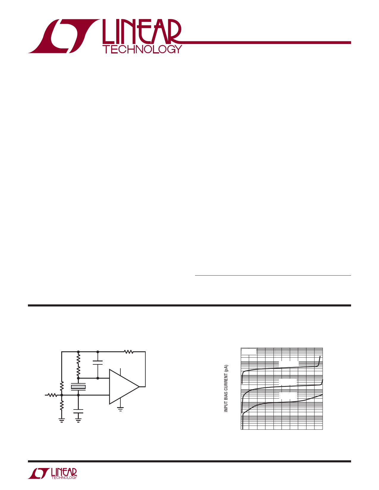
TYPICAL APPLICATION
Shock Sensor Amplifier
200k
100k
3V
2k
20M
20M
*
470pF
3V
–
1/2
LTC6084
+
VOUT = 120mV/g
100k
0.22μF
7Hz TO 5kHz
60845 TA01
*SHOCK SENSOR MURATA ERIE PKGS-OOMX1
www.murata.com
Input Bias Current
vs Common Mode Voltage
10000
VS = 5V
1000
TA = 125°C
100
TA = 85°C
10
TA = 25°C
1
0.1
0.01
0 0.5 1 1.5 2 2.5 3 3.5 4 4.5 5
COMMON MODE VOLTAGE (V)
60845 TA01b
60845fa
1
1 page 
LTC6084/LTC6085
ELECTRICAL CHARACTERISTICS The l denotes the specifications which apply over the full operating
temperature range, otherwise specifications are at TA = 25°C. Test conditions are V+ = 5V, V– = 0V, VCM = 0.5V unless otherwise noted.
C SUFFIX
H SUFFIX
SYMBOL PARAMETER
CONDITIONS
MIN TYP MAX MIN TYP MAX UNITS
CMRR
Common Mode Rejection 0 ≤ VCM ≤ 5V
Ratio
70
l 68
84
70 84
66
dB
dB
PSRR
Power Supply Rejection VS = 2.5V to 5.5V
Ratio
94
l 91
115
94 115
89
dB
dB
VOUT Output Voltage, High, No Load
(Referred to V+)
ISOURCE = 1mA
ISOURCE = 5mA
l 0.5 5
l 39 85
l 220 460
0.5 10
39 100
220
mV
mV
mV
Output Voltage, Low,
(Referred to V–)
No Load
ISINK = 1mA
ISINK = 5mA
l 0.5 5
l 36 85
l 200 460
0.5 10
36 100
200
mV
mV
mV
AVOL Large-Signal Voltage Gain RLOAD = 10k, 0.5V ≤ VOUT ≤ 4.5V
1000 5000
l 400
1000 5000
300
V/mV
V/mV
ISC
Output Short-Circuit
Source and Sink
Current
7.7
l6
12.5
7.7 12.5
4.5
mA
mA
SR
GBW
Φ0
tS
IS
Slew Rate
Gain Bandwidth Product
(fTEST = 10kHz)
Phase Margin
Settling Time 0.1%
Supply Current
(Per Amplifier)
AV = 1
RLOAD = 50k, VCM = 2.5V
RL = 10k, CL = 150pF, AV = 1
VSTEP = 1V, AV = 1
No Load
0.5 0.5
0.9
l 0.7
1.5
0.9 1.5
0.6
45 45
55
110 130
l 140
110 130
145
V/μs
MHz
Deg
μs
μA
μA
Shutdown Current
(Per Amplifier)
Shutdown, VSHDNx ≤ 1.2V
l
1.1 1.8
1.1 2
μA
VS
Supply Voltage Range Guaranteed by the PSRR Test
l 2.5
5.5 2.5
5.5 V
Channel Separation
Shutdown Logic
fS = 10kHz
SHDNx High
SHDNx Low
–120
3.5
1.2
–120
3.5
1.2
dB
V
V
tON Turn On Time
VSHDNx = 1.2V to 3.5V
tOFF Turn Off Time
VSHDNx = 3.5V to 1.2V
Leakage of SHDN Pin
VSHDNx = 0V
l
7
1
0.5 0.9
7
1
0.5 1.2
μs
μs
μA
Note 1: Stresses beyond those listed under Absolute Maximum Ratings
may cause permanent damage to the device. Exposure to any Absolute
Maximum Rating condition for extended periods may affect device
reliability and lifetime.
Note 2: A heat sink may be required to keep the junction temperature
below the absolute maximum. This depends on the power supply voltage
and the total output current.
Note 3: The LTC6084C/LTC6085C are guaranteed functional over the
operating temperature range of –40°C to 85°C. The LTC6084H/LTC6085H
are guaranteed functional over the operating temperature range of –40°C
to 125°C.
Note 4: The LTC6084C/LTC6085C are guaranteed to meet specified
performance from 0°C to 70°C. The LTC6084C/LTC6085C are designed,
characterized and expected to meet specified performance from –40°C
to 85°C but are not tested or QA sampled at these temperatures. The
LTC6084H/LTC6085H are guaranteed to meet specified performance from
–40°C to 125°C.
Note 5: ESD (Electrostatic Discharge) sensitive device. ESD protection
devices are used extensively internal to the LTC6084/LTC6085; however,
high electrostatic discharge can damage or degrade the device. Use proper
ESD handling precautions.
Note 6: This parameter is not 100% tested.
Note 7: This specification is limited by high speed automated test
capability. See Typical Performance Characteristic curves for actual
performance.
Note 8: Current noise is calculated from in = √2qIB, where q = 1.6 • 10–19
coulombs.
60845fa
5
5 Page 
LTC6084/LTC6085
APPLICATIONS INFORMATION
SHDN Pins
Pins 5 and 6 are used for power shutdown of the LTC6084
in the DD package. If they are floating, internal current
sources pull pins 5 and 6 to V+ and the amplifiers operate
normally. In shutdown the amplifier output is high imped-
ance, and each amplifier draws less than 1μA current.
This feature allows the part to be used in muxed output
applications as shown in Figure 3.
10k
5V
10k
INA
10k
5V
+
A
– SHDN
A
10k
LTC6084
(DD PACKAGE)
10k
5V
10k
INB
10k
SEL
+
B
–
OUT
SEL = 5V, OUT = –INA
SEL = 0V, OUT = –INB
10k
5V SHDN
B
FAIRCHILD
NC7SZ04 OR
EQUIVALENT 60845 F03
Figure 3. Inverting Amplifier with Muxed Output
ESD
The LTC6084/LTC6085 has reverse-biased ESD protection
diodes on all inputs and outputs as shown in the Simpli-
fied Schematic. If these pins are forced beyond either
supply, unlimited current will flow through these diodes.
If the current is transient and limited to 100mA or less,
no damage to the device will occur.
The amplifier input bias current is the leakage current of
these ESD diodes. This leakage is a function of the tem-
perature and common mode voltage of the amplifier, as
shown in the Typical Performance Characteristics.
Noise
In the frequency region above 1kHz, the LTC6084/LTC6085
shows good noise voltage performance. In this region,
noise can be dominated by the total source resistance of the
particular application. Specifically, these amplifiers exhibit
the noise of a 58k resistor, meaning it is desirable to keep
the source and feedback resistance at or below this value,
i.e., RS + RG||RFB ≤ 58k. Above this total source impedance,
the noise voltage is dominated by the resistors.
At low frequency, noise current can be estimated from the
expression in = √2qIB, where q = 1.6 • 10–19 coulombs.
Equating √4kTRΔf and R√2qIBΔf shows that for a source
resistor below 50GΩ the amplifier noise is dominated by
the source resistance. Noise current rises with frequency.
See the curve Input Noise Current vs Frequency in the
Typical Performance Characteristics section.
60845fa
11
11 Page | ||
| Páginas | Total 16 Páginas | |
| PDF Descargar | [ Datasheet LTC6085.PDF ] | |
Hoja de datos destacado
| Número de pieza | Descripción | Fabricantes |
| LTC6081 | (LTC6081 / LTC6082) Precision Quad CMOS Rail-to-Rail Input/Output Amplifier | Linear Technology |
| LTC6082 | (LTC6081 / LTC6082) Precision Quad CMOS Rail-to-Rail Input/Output Amplifier | Linear Technology |
| LTC6084 | CMOS Amplifiers | Linear |
| LTC6085 | CMOS Amplifiers | Linear |
| Número de pieza | Descripción | Fabricantes |
| SLA6805M | High Voltage 3 phase Motor Driver IC. |
Sanken |
| SDC1742 | 12- and 14-Bit Hybrid Synchro / Resolver-to-Digital Converters. |
Analog Devices |
|
DataSheet.es es una pagina web que funciona como un repositorio de manuales o hoja de datos de muchos de los productos más populares, |
| DataSheet.es | 2020 | Privacy Policy | Contacto | Buscar |