|
|
|
PDF XP1017-BD Data sheet ( Hoja de datos )
| Número de pieza | XP1017-BD | |
| Descripción | Power Amplifier | |
| Fabricantes | Mimix Broadband | |
| Logotipo | ||
Hay una vista previa y un enlace de descarga de XP1017-BD (archivo pdf) en la parte inferior de esta página. Total 8 Páginas | ||
|
No Preview Available !
30.0-36.0 GHz GaAs MMIC
Power Amplifier
January 2010 - Rev 23-Jan-10
P1017-BD
Features
Balanced Design Provides Good Input/Output Match
On-Chip Temperature Compensated Output
Power Detector
16.0 dB Small Signal Gain
+33.0 dBm Third Order Intercept (OIP3)
100% On-Wafer RF, DC and Output Power Testing
100% Visual Inspection to MIL-STD-883
Method 2010
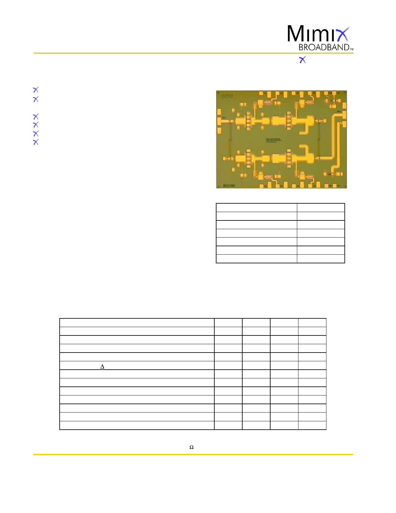
Chip Device Layout
XP1017-BD
General Description
Mimix Broadband’s two stage 30.0-36.0 GHz GaAs
MMIC power amplifier is optimized for linear operation
with a third order intercept point of +33.0 dBm.The
device also includes Lange couplers to achieve good
input/output return loss and an on-chip temperature
compensated output power detector.This MMIC uses
Mimix Broadband’s GaAs PHEMT device model
technology, and is based upon electron beam
lithography to ensure high repeatability and uniformity.
The chip has surface passivation to protect and provide
a rugged part with backside via holes and gold
metallization to allow either a conductive epoxy or
eutectic solder die attach process.This device is well
suited for Millimeter-wave Point-to-Point Radio, LMDS,
SATCOM and VSAT applications.
Absolute Maximum Ratings
Supply Voltage (Vd)
Supply Current (Id)
Gate Bias Voltage
Input Power (Pin)
Storage Temperature (Tstg)
Operating Temperature (Ta)
Channel Temperature (Tch)1
+6.0 VDC2
950 mA
+0.3 VDC
+15 dBm
-65 to +165 ºC
-55 to +85ºC
+175 ºC
(1) Channel temperature affects a device's MTTF. It is
recommended to keep channel temperature as low as
possible for maximum life.
(2) Under pulsed bias conditions, under CW Psat conditions
further reduction in max supply voltage (~0.5V) is
recommended.
Electrical Characteristics (Ambient Temperature T = 25 oC)
Parameter
Units
Frequency Range (f )
GHz
Input Return Loss (S11)
dB
Output Return Loss (S22)
dB
Small Signal Gain (S21)
dB
Gain Flatness ( S21)
dB
Reverse Isolation (S12)
Output Power for 1 dB Compression (P1dB) 2
Output Third Order Intercept Point (OIP3)1,2
dB
dBm
dBm
Drain Bias Voltage (Vd1,2,3,4)
VDC
Gate Bias Voltage (Vg1,2,3,4)
VDC
Supply Current (Id) (Vd=4.5V, Vg=-0.7V Typical)
Detector (diff ) Output at 20 dBm3
mA
VDC
(1) Measured at +17 dBm per tone output carrier level across the full frequency band.
(2) Measured using constant current.
(3) Measured with either Vin=1.0V or Vin=5.5V and Rin=5.6k .
Min.
30.0
-
-
-
-
-
-
-
-
-1.0
-
-
Typ.
-
16.0
20.0
16.0
+/-0.5
40.0
+24.0
+33.0
+4.5
-0.7
440
0.3
Max.
36.0
-
-
-
-
-
-
-
+5.5
0.0
880
-
Mimix Broadband, Inc., 10795 Rockley Rd., Houston, Texas 77099
Tel: 281.988.4600 Fax: 281.988.4615 mimixbroadband.com
Page 1 of 8
Characteristic Data and Specifications are subject to change without notice. ©2010 Mimix Broadband, Inc.
Export of this item may require appropriate export licensing from the U.S. Government. In purchasing these parts, U.S. Domestic customers accept
their obligation to be compliant with U.S. Export Laws.
1 page 
30.0-36.0 GHz GaAs MMIC
Power Amplifier
January 2010 - Rev 23-Jan-10
Mechanical Drawing
2.500
(0.098)
1.141 1.541 1.941 2.341 2.741 2.941
(0.045) (0.061) (0.076) (0.092) (0.108) (0.116)
2 3 4 5 67
P1017-BD
1.710
(0.067)
1
XP1017-BD
8
1.851
(0.073)
0.0 14 13 12 11 10 9
0.0 1.141 1.541 1.941 2.341 2.741 2.941 3.300
(0.045) (0.061) (0.076) (0.092) (0.108) (0.116) (0.130)
(Note: Engineering designator is 32H2BA0070)
Units: millimeters (inches) Bond pad dimensions are shown to center of bond pad.
Thickness: 0.110 +/- 0.010 (0.0043 +/- 0.0004), Backside is ground, Bond Pad/Backside Metallization: Gold
All DC Bond Pads are 0.100 x 0.100 (0.004 x 0.004). All RF Pads are 0.100 x 0.200 (0.004 x 0.008).
Bond pad centers are approximately 0.109 (0.004) from the edge of the chip.
Dicing tolerance: +/- 0.005 (+/- 0.0002). Approximate weight: 5.115 mg.
Bond Pad #1 (RF In)
Bond Pad #2 (Vg1)
Bond Pad #3 (Vd2)
Bias Arrangement
Vd1,2
Bond Pad #4 (Vg2)
Bond Pad #5 (Vd2)
Bond Pad #6 (VDIF1)
Bond Pad #7 (VIN2)
Bond Pad #8 (RF Out)
Bond Pad #9 (VIN1)
Bond Pad #10 (VDIF2)
Bond Pad #11 (Vd4)
Bond Pad #12 (Vg4)
Bond Pad #13 (Vd3)
Bond Pad #14 (Vg3)
Bypass Capacitors - See App Note [3]
Vg1,2
VDIF2
VIN2
2 3 4 5 67
RF In 1
XP1017-BD
8 RF Out
14 13 12 11 10 9
Vg3,4
Vd3,4
VIN1
VDIF1
Mimix Broadband, Inc., 10795 Rockley Rd., Houston, Texas 77099
Tel: 281.988.4600 Fax: 281.988.4615 mimixbroadband.com
Page 5 of 8
Characteristic Data and Specifications are subject to change without notice. ©2010 Mimix Broadband, Inc.
Export of this item may require appropriate export licensing from the U.S. Government. In purchasing these parts, U.S. Domestic customers accept
their obligation to be compliant with U.S. Export Laws.
5 Page | ||
| Páginas | Total 8 Páginas | |
| PDF Descargar | [ Datasheet XP1017-BD.PDF ] | |
Hoja de datos destacado
| Número de pieza | Descripción | Fabricantes |
| XP1017-BD | Power Amplifier | Mimix Broadband |
| Número de pieza | Descripción | Fabricantes |
| SLA6805M | High Voltage 3 phase Motor Driver IC. |
Sanken |
| SDC1742 | 12- and 14-Bit Hybrid Synchro / Resolver-to-Digital Converters. |
Analog Devices |
|
DataSheet.es es una pagina web que funciona como un repositorio de manuales o hoja de datos de muchos de los productos más populares, |
| DataSheet.es | 2020 | Privacy Policy | Contacto | Buscar |