|
|
PDF VND5004ASP30-E Data sheet ( Hoja de datos )
| Número de pieza | VND5004ASP30-E | |
| Descripción | high-side driver | |
| Fabricantes | STMicroelectronics | |
| Logotipo |  |
|
Hay una vista previa y un enlace de descarga de VND5004ASP30-E (archivo pdf) en la parte inferior de esta página. Total 30 Páginas | ||
|
No Preview Available !
VND5004A-E
VND5004ASP30-E
Double 4mΩ high side driver with analog current sense
for automotive applications
Features
Max transient supply voltage
Operating voltage range
Max On-State resistance (per ch.)
Current limitation (typ)
Off state supply current
VCC
VCC
RON
ILIMH
IS
41V
4.5 to 27V
4 mΩ
100A
2 µA(1)
PQFN - 12x12 Power lead-less
MultiPowerSO-30
1. Typical value with all loads connected
Application
■ General
– Inrush current active management by
power limitation
– Very low stand-by current
– 3.0V CMOS compatible input
– Optimized electromagnetic emission
– Very low electromagnetic susceptibility
– In compliance with the 2002/95/EC
European directive
■ Diagnostic functions
– Proportional load current sense
– Current sense disable
– Thermal shutdown indication
■ Protection
– Undervoltage shut-down
– Overvoltage clamp
– Load current limitation
– Thermal shut down
– Self limiting of fast thermal transients
– Protection against loss of ground and loss of VCC
– Reverse battery protection with self switch
on of the PowerMOS (see Application
schematic on page 18)
– Electrostatic discharge protection
Table 1. Devices summary
■ All types of resistive, inductive and capacitive
loads
■ Suitable for power management applications
Description
The VND5004ATR-E and VND5004ASP30-E are
devices made using STMicroelectronics VIPower
technology. They are intended for driving resistive
or inductive loads with one side connected to
ground. Active VCC pin voltage clamp and load
dump protection circuit protect the devices
against transients on the Vcc pin (see ISO7637
transient compatibility table). These devices
integrate an analog current sense which delivers
a current proportional to the load current
(according to a known ratio) when CS_DIS is
driven low or left open. When CS_DIS is driven
high, the CURRENT SENSE pin is high
impedance. Output current limitation protects the
devices in overload condition. In case of long
duration overload, the devicesa limit the
dissipated power to a safe level up to thermal
shut-down intervention. Thermal shut-down with
automatic restart allows the device to recover
normal operation as soon as a fault condition
disappears.
Package
Tube
Order codes
Tape and Reel
Tray
PQFN-12x12 Power lead-less
-
VND5004ATR-E
VND5004A-E
MultiPowerSO-30
VND5004ASP30-E
VND5004ASP30TR-E
-
December 2007
Rev 5
1/34
www.st.com
34
1 page 
VND5004A-E / VND5004ASP30-E
Block diagram and pin configurations
1 Block diagram and pin configurations
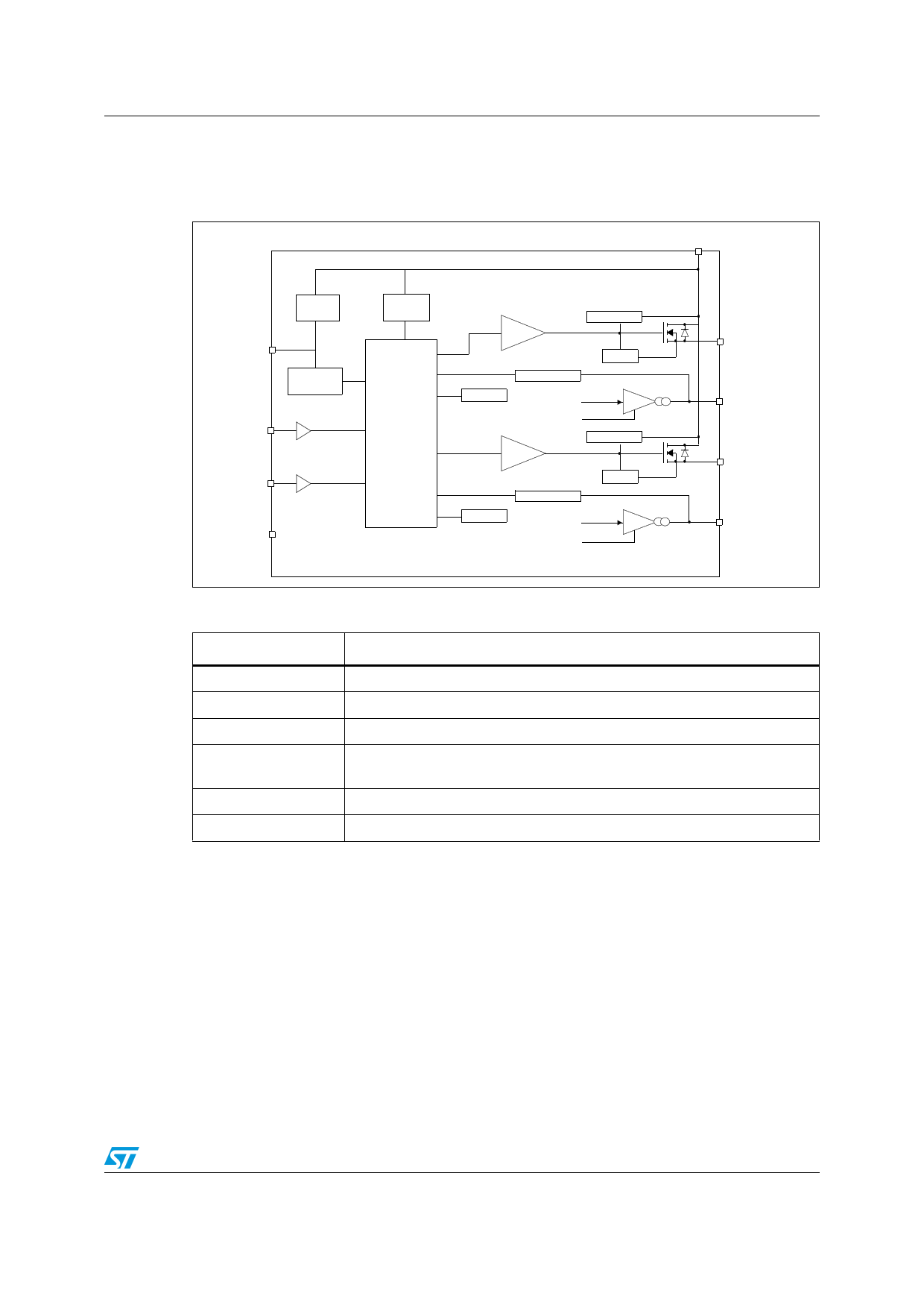
Figure 1. Block diagram
VCC
GND
VCC
clamp
Rbpareotvtteeercrystieon
INPUT1
Under
voltage
LOGIC
INPUT2
CS_DIS
DRIVER
PwCLAMP
PwrLIM
Overtemp.
ILIM
IOUT1
K
CS_DIS
DRIVER
PwCLAMP
PwrLIM
Overtemp.
ILIM
IOUT2
K
CS_DIS
OUTPUT1
CURRENT
SENSE1
OUTPUT2
CURRENT
SENSE2
Table 2. Pin functions
Name
Function
VCC
Battery connection
OUTPUT1,2
Power output
GND
Ground connection
INPUT1,2
Voltage controlled input pin with hysteresis, CMOS compatible. Controls
output switch state
CURRENT SENSE1,2 Analog current sense pin, delivers a current proportional to the load current
CS_DIS
Active high CMOS compatible pin, to disable the current sense pins
5/34
5 Page 
VND5004A-E / VND5004ASP30-E
Electrical specifications
Table 10. Current sense (8V<VCC<16V)
Symbol
Parameter
Test conditions
Min. Typ. Max. Unit
K1
K2
ISENSE0
VSENSE
IOUT/ISENSE
IOUT/ISENSE
Analog sense
current
Max analog sense
output voltage
IOUT=15A; VSENSE=4V; VCSD=0V;
Tj=-40°C
Tj=25°C...150°C
11530 16000 19340
12730 16000 19270
IOUT=30A; VSENSE=4V; VCSD=0V;
Tj=-40°C
Tj=25°C...150°C
13430 16150 17880
14500 16150 17880
IOUT=0A; VSENSE=0V;
VCSD=5V; VIN=0V; Tj=-40°C to 150°C
VCSD=0V; VIN=5V; Tj=-40°C to 150°C
0
0
5 µA
400 µA
IOUT=45A; VCSD=0V; RSENSE=3.9kΩ 5
V
VSENSEH
Analog sense
output voltage in
overtemperature
condition
VCC=13V; RSENSE=3.9kΩ
9V
ISENSEH
Analog sense
output current in
overtemperature
condition
Vcc=13V; VSENSE=5V
8 mA
Delay response
tDSENSE1H
time from falling
edge of CS_DIS
pin
VSENSE<4V, 5A<Iout<30A
ISENSE=90% of ISENSE max
(see Figure 4.)
50 100 µs
Delay response
tDSENSE1L
time from rising
edge of CS_DIS
pin
VSENSE<4V, 5A<Iout<30A
ISENSE=10% of ISENSE max
(see Figure 4.)
5 20 µs
Delay response
tDSENSE2H time from rising
edge of INPUT pin
VSENSE<4V, 5A<Iout<30A
ISENSE=90% of ISENSE max
(see Figure 4.)
Delay response
tDSENSE2L time from falling
edge of INPUT pin
VSENSE<4V, 5A<Iout<30A
ISENSE=10% of ISENSE max
(see Figure 4.)
270 600 µs
100 250 µs
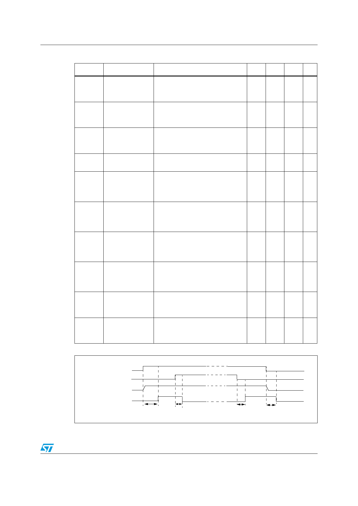
Figure 4. Current sense delay characteristics
INPUT
CS_DIS
LOAD CURRENT
SENSE CURRENT
tDSENSE2H tDSENSE1L
tDSENSE1H tDSENSE2L
11/34
11 Page | ||
| Páginas | Total 30 Páginas | |
| PDF Descargar | [ Datasheet VND5004ASP30-E.PDF ] | |
Hoja de datos destacado
| Número de pieza | Descripción | Fabricantes |
| VND5004ASP30-E | high-side driver | STMicroelectronics |
| Número de pieza | Descripción | Fabricantes |
| SLA6805M | High Voltage 3 phase Motor Driver IC. |
Sanken |
| SDC1742 | 12- and 14-Bit Hybrid Synchro / Resolver-to-Digital Converters. |
Analog Devices |
|
DataSheet.es es una pagina web que funciona como un repositorio de manuales o hoja de datos de muchos de los productos más populares, |
| DataSheet.es | 2020 | Privacy Policy | Contacto | Buscar |
