|
|
|
PDF P4C164LL Data sheet ( Hoja de datos )
| Número de pieza | P4C164LL | |
| Descripción | STATIC CMOS RAM | |
| Fabricantes | PYRAMID | |
| Logotipo | ||
Hay una vista previa y un enlace de descarga de P4C164LL (archivo pdf) en la parte inferior de esta página. Total 10 Páginas | ||
|
No Preview Available !
FEATURES
VCC Current (Commercial/Industrial)
— Operating: 55 mA
— CMOS Standby: 3 µA
Access Times
—80/100 (Commercial or Industrial)
—90/120 (Military)
Single 5 Volts ±10% Power Supply
Easy Memory Expansion Using CE1, CE2 and OE
Inputs
P4C164LL
VERY LOW POWER 8Kx8
STATIC CMOS RAM
Common Data I/O
Three-State Outputs
Fully TTL Compatible Inputs and Outputs
Advanced CMOS Technology
Automatic Power Down
Packages
—28-Pin 300 and 600 mil DIP
—28-Pin 330 mil SOP
DESCRIPTION
The P4C164LL is a 64K density low power CMOS static
RAM organized as 8Kx8. The CMOS memory requires
no clocks or refreshing, and has equal access and cycle
times. Inputs are fully TTL-compatible. The RAM operates
from a single 5V±10% tolerance power supply.
Access times of 80 and 100 ns are available for commercial
and industrial temperatures; access times of 90 and 100
ns are available for military temperature. CMOS is utilized
to reduce power consumption to a low level.
The P4C164LL device provides asynchronous operation
with matching access and cycle times.
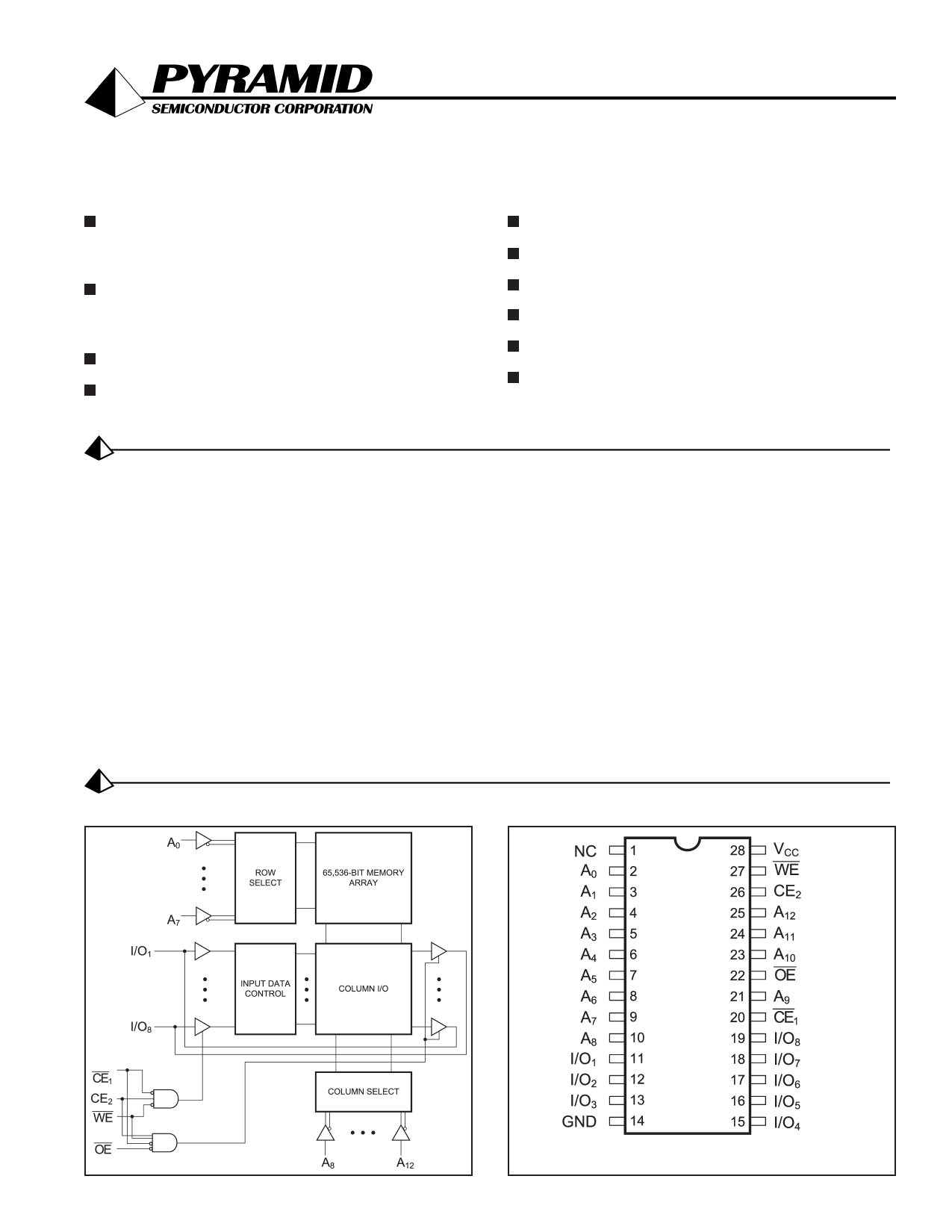
Memory locations are specified on address pins A0 to A12.
Reading is accomplished by device selection (CE1 LOW,
CE2 HIGH ) and output enabling (OE) while write enable
(WE) remains HIGH. By presenting the address under
these conditions, the data in the addressed memory loca-
tion is presented on the data input/output pins. The input/
output pins stay in the HIGH Z state when either CE1 or
OE is HIGH or WE or CE2 is LOW.
Package options for the P4C164LL include 28-pin 300 and
600 mil DIP and 28-pin 330 mil SOP packages.
Functional Block Diagram
Pin ConfigurationS
Document # SRAM116 REV 04
DIP (P5, P6, C5-1), SOP (S5)
TOP VIEW
Revised June 2014
1 page 
AC CHARACTERISTICS—WRITE CYCLE
(Over Recommended Operating Temperature & Supply Voltage)
Symbol Parameter
-80
Min Max
tWC Write Cycle Time
80
tCW Chip Enable Time to End of Write
70
tAW Address Valid to End of Write
tAS Address Setup Time
70
0
tWP Write Pulse Width
tAH Address Hold Time
60
0
tDW Data Valid to End of Write
40
tDH Data Hold Time
tWZ Write Enable to Output in High Z
0
30
tOW Output Active from End of Write
10
P4C164LL - VERY LOW POWER 8K x 8 STATIC CMOS RAM
-90
Min Max
90
80
80
0
60
0
40
0
30
10
-100
Min Max
100
80
80
0
60
0
40
0
30
10
-120
Min Max
120
100
100
0
60
0
40
0
30
10
Unit
ns
ns
ns
ns
ns
ns
ns
ns
ns
ns
TIMING WAVEFORM OF WRITE Cycle No. 1 (WE Controlled)(6)
Notes:
11. CE1 and WE must be LOW, and CE2 HIGH for WRITE cycle.
12. OE is LOW for this WRITE cycle to show tWZ and tOW.
13. If CE1 goes HIGH, or CE2 goes LOW, simultaneously with WE HIGH,
the output remains in a high impedance state
14. Write Cycle Time is measured from the last valid address to the first
transitioning address.
Document # SRAM116 REV 04
Page 5
5 Page | ||
| Páginas | Total 10 Páginas | |
| PDF Descargar | [ Datasheet P4C164LL.PDF ] | |
Hoja de datos destacado
| Número de pieza | Descripción | Fabricantes |
| P4C164LL | STATIC CMOS RAM | PYRAMID |
| Número de pieza | Descripción | Fabricantes |
| SLA6805M | High Voltage 3 phase Motor Driver IC. |
Sanken |
| SDC1742 | 12- and 14-Bit Hybrid Synchro / Resolver-to-Digital Converters. |
Analog Devices |
|
DataSheet.es es una pagina web que funciona como un repositorio de manuales o hoja de datos de muchos de los productos más populares, |
| DataSheet.es | 2020 | Privacy Policy | Contacto | Buscar |