|
|
PDF X9118 Data sheet ( Hoja de datos )
| Número de pieza | X9118 | |
| Descripción | Single Digitally Controlled Potentiometer | |
| Fabricantes | Intersil | |
| Logotipo |  |
|
Hay una vista previa y un enlace de descarga de X9118 (archivo pdf) en la parte inferior de esta página. Total 17 Páginas | ||
|
No Preview Available !
X9118
Dual Supply/Low Power/1024-Tap/2-Wire Bus
Data Sheet
April 9, 2014
FN8161.5
Single Digitally-Controlled (XDCP™)
Potentiometer
The X9118 is a single digitally controlled potentiometer
(XDCP) on a monolithic CMOS integrated circuit.
The digital controlled potentiometer is implemented using
1023 resistive elements in a series array. Between each
element are tap points connected to the wiper terminal
through switches. The position of the wiper on the array is
controlled by the user through the 2-wire bus interface. The
potentiometer has associated with it a volatile Wiper Counter
Register (WCR) and a four non-volatile Data Registers that
can be directly written to and read by the user. The contents
of the WCR controls the position of the wiper on the resistor
array though the switches. Power-up recalls the contents of
the default data register (DR0) to the WCR.
The XDCP can be used as a three-terminal potentiometer or
as a two terminal variable resistors in a wide variety of
applications including control, parameter adjustments, and
signal processing.
Features
• 1024 resistor taps – 10-bit resolution
• 2-wire serial interface for write, read and transfer
operations of the potentiometer
• Wiper resistance, 40Ω typical @ 5V
• Four non-volatile data registers for each potentiometer
• Non-volatile storage of multiple wiper positions
• Power on recall: Loads saved wiper position on power-up
• Standby current < 15µA Max
• System VCC: 2.7V to 5.5V operation
• Analog V+/V-: -5V to +5V
• 100kΩ end-to-end resistance
• Endurance: 100,000 data changes per bit per register
• 100 years data retention
• 14 Ld TSSOP
• Low power CMOS
• Pb-free (RoHS compliant)
Ordering Information
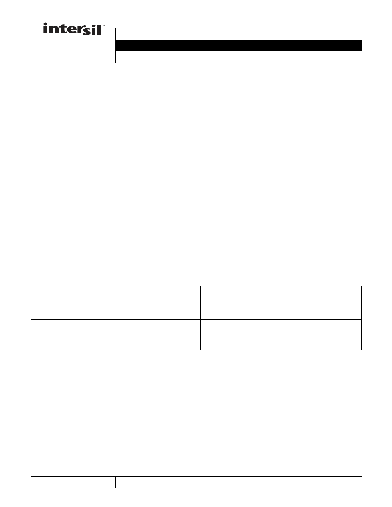
PART NUMBER
(Notes 1, 2)
PART
MARKING
VCC LIMITS
(V)
POTENTIOMETER
ORGANIZATION
(kΩ)
TEMP
RANGE
(°C)
PACKAGE
(Pb-free)
PKG.
DWG. #
X9118TV14IZ
X9118 TVZI
5 ±10%
100 -40 to +85 14 Ld TSSOP M14.173
X9118TV14IZ-2.7
X9118 TVZG
2.7 to 5.5
100 -40 to +85 14 Ld TSSOP M14.173
X9118TV14Z
X9118 TVZ
5 ±10%
100 0 to +70 14 Ld TSSOP M14.173
X9118TV14Z-2.7
X9118 TVZF
2.7 to 5.5
100 0 to +70 14 Ld TSSOP M14.173
NOTES:
1. These Intersil Pb-free plastic packaged products employ special Pb-free material sets, molding compounds/die attach materials, and 100% matte
tin plate plus anneal (e3 termination finish, which is RoHS compliant and compatible with both SnPb and Pb-free soldering operations). Intersil
Pb-free products are MSL classified at Pb-free peak reflow temperatures that meet or exceed the Pb-free requirements of IPC/JEDEC J STD-
020.
2. For Moisture Sensitivity Level (MSL), please see product information page for X9118. For more information on MSL, please see tech brief TB363.
1 CAUTION: These devices are sensitive to electrostatic discharge; follow proper IC Handling Procedures.
1-888-INTERSIL or 1-888-468-3774 | Copyright Intersil Americas LLC 2005, 2008, 2009, 2014. All Rights Reserved
Intersil (and design) and XDCP are trademarks owned by Intersil Corporation or one of its subsidiaries.
All other trademarks mentioned are the property of their respective owners.
1 page 
X9118
SCL FROM
MASTER
DATA OUTPUT
FROM TRANSMITTER
1
89
DATA OUTPUT
FROM RECEIVER
START
FIGURE 2. ACKNOWLEDGE RESPONSE FROM RECEIVER
ACKNOWLEDGE
ACKNOWLEDGE POLLING
The disabling of the inputs during the internal nonvolatile write
operation, can be used to take advantage of the typical 5ms
EEPROM write cycle time. Once the stop condition is issued to
indicate the end of the nonvolatile write command the X9118
initiates the internal write cycle. The ACK polling, Flow 1, can
be initiated immediately. This involves issuing the start
condition followed by the device slave address. If the X9118 is
still busy with the write operation no ACK will be returned. If the
X9118 has completed the write operation an ACK will be
returned and the master can then proceed with the next
operation.
Flow 1. ACK Polling Sequence
NONVOLATILE WRITE
COMMAND COMPLETED
ENTERACK POLLING
ISSUE
START
ISSUE SLAVE
ADDRESS
ISSUE STOP
ACK
RETURNED?
YES
NO
INSTRUCTION AND REGISTER DESCRIPTION
Device Addressing: Identification Byte (ID and A)
Following a start condition, the master must output the
address of the slave it is accessing. The most significant
4 bits of the slave address are the device type identifier. The
ID[3:0] bits is the device ID for the X9118; this is fixed as
0101[B] (refer to Table 1 on page 6).
The A[1:0] bits in the ID byte are the internal slave address.
The physical device address is defined by the state of the
A1-A0 input pins. The slave address is externally specified
by the user. The X9118 compares the serial data stream with
the address input state; a successful compare of both
address bits is required for the X9118 to successfully
continue the command sequence. Only the device which
slave address matches the incoming device address sent by
the master executes the instruction. The A1 to A0 inputs can
be actively driven by CMOS input signals or tied to VCC or
VSS. The R/W bit is the LSB and used to set the device for
read or write operations.
INSTRUCTION BYTE AND REGISTER SELECTION
The next byte sent to the X9118 contains the instruction and
register pointer information. The three most significant bits
are used to provide the instruction opcode (I[2:0]). The RB
and RA bits point to one of the four registers. The format is
shown in Table 2.
Table 3 provides a complete summary of the instruction set
opcodes.
FURTHER
OPERATION?
NO
YES
ISSUE
INSTRUCTION
ISSUE STOP
PROCEED
PROCEED
Submit Document Feedback
5
FN8161.5
April 9, 2014
5 Page 
X9118
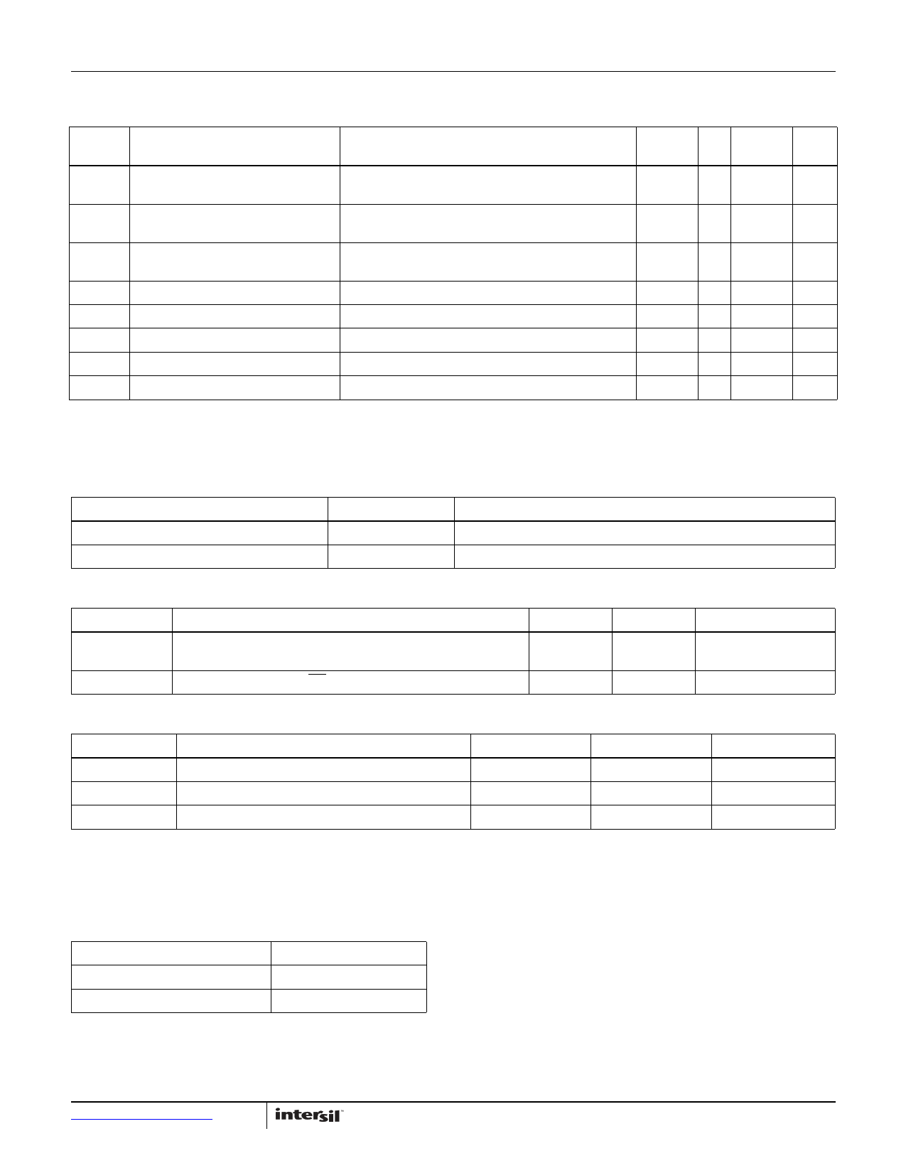
DC Operating Specifications TA = +25°C, unless otherwise noted. Boldface limits apply across the operating temperature range ,
-40°C to +85°C.
SYMBOL
PARAMETER
TEST CONDITIONS
MIN MAX
(Note 10) TYP (Note 10) UNITS
ICC1 VCC Supply Current (Active)
fSCL = 400kHz; VCC = +5.5V; SDA = Open;
(for 2-wire, Active, Read and Volatile Write States only)
3 mA
ICC2
VCC Supply Current (Nonvolatile Write) fSCL = 400kHz; VCC = +5.5V; SDA = Open;
(for 2-wire, Active, Non-volatile Write State only)
7 mA
ISB VCC Current (Standby)
VCC = +5.5V; VIN = VSS or VCC; SDA = VCC;
(for 2-wire, Standby State only)
15 μA
ILI Input Leakage Current
VIN = VSS to VCC
10 μA
ILO Output Leakage Current
VOUT = VSS to VCC
10 μA
VIH Input HIGH Voltage
VCC x 0.7
VCC + 1
V
VIL Input LOW Voltage
-1 VCC x 0.3 V
VOL Output LOW Voltage
IOL = 3mA
0.4 V
NOTE:
10. Parameters with MIN and/or MAX limits are 100% tested at +25°C, unless otherwise specified. Temperature limits established by characterization
and are not production tested.
Endurance and Data Retention
PARAMETER
Minimum Endurance
Data Retention
MIN
100,000
100
UNITS
Data changes per bit per register
years
Capacitance
SYMBOL
CIN/OUT
(Note 11)
CIN (Note 11)
TEST
Input/Output Capacitance (SI)
Input Capacitance (SCL, WP, A1 and A0)
TYP
8
6
UNITS
pF
pF
TEST CONDITIONS
VOUT = 0V
VIN = 0V
Power-Up Timing
SYMBOL
PARAMETER
MIN
MAX
UNITS
tr VCC (Note 11) VCC Power-up Rate
0.2 50 V/ms
tPUR (Note 12) Power-up to Initiation of Read Operation
1 ms
tPUW (Note 12) Power-up to Initiation of Write Operation
50 ms
NOTES:
11. This parameter is not 100% tested.
12. tPUR and tPUW are the delays required from the time the (last) power supply (VCC-) is stable until the specific instruction can be issued. These
parameters are periodically sampled and not 100% tested.
AC Test Conditions
Input Pulse Levels
Input Rise and Fall Times
Input and Output Timing Level
VCC x 0.1 to VCC x 0.9
10ns
VCC x 0.5
Submit Document Feedback 11
FN8161.5
April 9, 2014
11 Page | ||
| Páginas | Total 17 Páginas | |
| PDF Descargar | [ Datasheet X9118.PDF ] | |
Hoja de datos destacado
| Número de pieza | Descripción | Fabricantes |
| X9110 | Single Digitally-Controlled (XDCP) Potentiometer | Xicor |
| X9110 | Single Digitally Controlled Potentiometer | Intersil |
| X9111 | Single Digitally-Controlled Potentiometer | Xicor |
| X9111 | Single Digitally Controlled Potentiometer | Intersil |
| Número de pieza | Descripción | Fabricantes |
| SLA6805M | High Voltage 3 phase Motor Driver IC. |
Sanken |
| SDC1742 | 12- and 14-Bit Hybrid Synchro / Resolver-to-Digital Converters. |
Analog Devices |
|
DataSheet.es es una pagina web que funciona como un repositorio de manuales o hoja de datos de muchos de los productos más populares, |
| DataSheet.es | 2020 | Privacy Policy | Contacto | Buscar |
