|
|
|
PDF FAN48630 Data sheet ( Hoja de datos )
| Número de pieza | FAN48630 | |
| Descripción | Synchronous TinyBoost Regulator | |
| Fabricantes | Fairchild Semiconductor | |
| Logotipo | ||
Hay una vista previa y un enlace de descarga de FAN48630 (archivo pdf) en la parte inferior de esta página. Total 15 Páginas | ||
|
No Preview Available !
November 2012
FAN48630 — 2.5 MHz, 1500 mA, Synchronous TinyBoost™
Regulator with Bypass Mode
Features
Few External Components: 0.47 µH Inductor and
0603 Case Size Input and Output Capacitors
Input Voltage Range: 2.35 V to 5.5 V
Fixed Output Voltage Options: 3.0 V to 5.0 V
Maximum Continuous Load Current: 1500 mA
at VIN of 2.6 V Boosting VOUT to 3.5 V
Up to 96% Efficient
True Bypass Operation when VIN > Target VOUT
Internal Synchronous Rectifier
Soft-Start with True Load Disconnect
Forced Bypass Mode
VSEL Control to Optimize Target VOUT
Short-Circuit Protection
Low Operating Quiescent Current
16-Bump, 0.4 mm Pitch WLCSP
Applications
Boost for Low-Voltage Li-ion Batteries, Brownout
Prevention, Boosted Audio, USB OTG, and LTE / 3G
RF Power
Cell Phones, Smart Phones, Portable Instruments
Description
The FAN48630 allows systems to take advantage of new
battery chemistries that can supply significant energy when
the battery voltage is lower than the required voltage for
system power ICs. By combining built-in power transistors,
synchronous rectification, and low supply current; this IC
provides a compact solution for systems using advanced
Li-Ion battery chemistries.
The FAN48630 is a boost regulator designed to provide a
minimum output voltage (VOUT(MIN)) from a single-cell Li-Ion
battery, even when the battery voltage is below system
minimum. Output voltage regulation is guaranteed to a
maximum load current of 1500 mA. Quiescent current in
Shutdown Mode is less than 3 µA, which maximizes battery
life. The regulator transitions smoothly between Bypass and
normal Boost Mode. The device can be forced into Bypass
Mode to reduce quiescent current.
The FAN48630 is available in a 16-bump, 0.4 mm pitch,
Wafer-Level Chip-Scale Package (WLCSP).
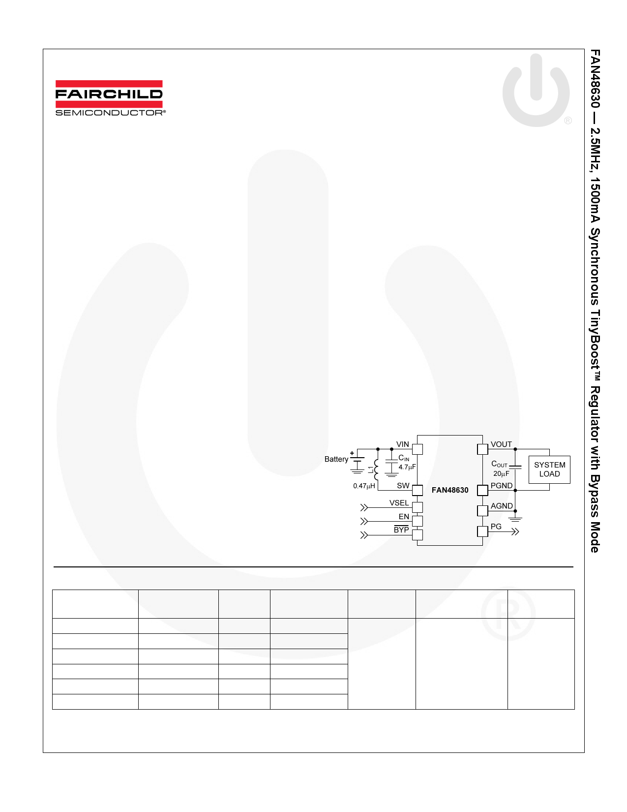
Figure 1. Typical Application
Ordering Information
Part Number
Output Voltage(1)
VSEL0 / VSEL1
Soft-
Start
Forced
Bypass
Operating
Temperature
Package(2)
FAN48630UC315X
FAN48630UC33X
FAN48630UC35X
FAN48630UC37AX
FAN48630UC45X
FAN48630UC50X
3.15 / 3.33
3.30 / 3.49
3.50 / 3.70
3.70 / 3.77
4.50 / 4.76
5.00 / 5.29
FAST
FAST
FAST
FAST
SLOW
SLOW
Low IQ
Low IQ
Low IQ
Low IQ
OCP On
OCP On
-40°C to 85°C
16-Ball, 4x4 Array,
0.4 mm Pitch,
250 µm Ball,
Wafer-Level Chip-
Scale Package
(WLCSP)
Notes:
1. Other output voltages are available on request. Please contact a Fairchild Semiconductor representative.
2. Includes backside laminate.
Packing
Tape and Reel
© 2011 Fairchild Semiconductor Corporation
FAN48630 • Rev. 1.0.1
www.fairchildsemi.com
1 page 
Electrical Specifications
Recommended operating conditions, unless otherwise noted, circuit per Figure 1, VIN = 2.35 V to VOUT, TA = -40˚C to 85˚C.
Typical values are given VIN = 3.0 V and TA = 25˚C.
Symbol
IQ
ILK
ILK_OUT
VUVLO
VUVLO_HYS
VPG(OL)
IPG_LK
VIH
VIL
RLOW
IPD
VREG
VTRSP
tON
fSW
IV_LIM
IV_LIM_SS
VMIN_1.5A
ISS_PK
tSS
VOCP
VOVP
VOVP_HYS
Parameter
VIN Quiescent Current
VOUT to VIN Reverse Leakage
VOUT Leakage Current
Under-Voltage Lockout
Under-Voltage Lockout Hysteresis
PG Low
PG Leakage Current
Logic Level HIGH EN, VSEL, BYP
Logic Level LOW EN, VSEL, BYP
Logic Control Pin Pull Downs
(LOW Active)
Weak Current Source Pull-Down
Output Voltage Accuracy
Load Transient Response
On-Time
Switching Frequency
Boost Valley Current Limit
Boost Valley Current Limit During
SS
Minimum VIN for 1500 mA Load
(Short Term)
Soft-Start Input Peak Current Limit
Soft-Start EN HIGH to Regulation
OCP Comparator Threshold
Output Over-Voltage Protection
Threshold
Output Over-Voltage Protection
Hysteresis
Conditions
Bypass Mode VOUT=3.5 V, VIN=4.2 V
Boost Mode VOUT=3.5 V, VIN=2.5 V
Shutdown: EN=0, VIN=3.0 V
Forced Bypass Mode
VOUT=3.5 V, VIN=3.5 V
Low IQ
OCP On
VOUT=5 V, EN=0
VOUT=0, EN=0, VIN=4.2 V
VIN Rising
IPG=5 mA
VPG=5 V
BYP, VSEL, EN
BYP, VSEL, EN
Referred to GND, DC, VOUT-VIN >
100 mV
500 – 1250 mA, VIN=3.6 V, VOUT=5.0 V
VIN=3.0 V, VOUT=3.5 V, Load >1000 mA
VIN=3.6 V, VOUT=5.0 V, Load=1000 mA
VIN=2.6 V
VIN=2.6 V
VOUT=5.0 V, TJ < 120˚C
VOUT=4.5 V, TJ < 120˚C
VOUT=3.5 V, TJ < 120˚C
VOUT=3.15 V, TJ < 120˚C
LIN1
Slow
Fast
LIN2
Slow
Fast
Slow, 50 Load
Fast, 50 Load
VIN=5.0 V, VIN-VOUT
Min.
1.2
Typ.
140
150
1.5
4
45
0.2
0.1
2.20
200
Max.
190
250
5.0
10
90
1.0
1.0
2.35
0.4
1
0.4
Unit
A
A
A
A
A
A
A
V
mV
V
µA
V
V
300 k
100 nA
–2 4 %
±4 %
80 ns
2.0 2.5 3.0 MHz
2.6 2.9 3.1
A
1.6 A
3.0
2.8
2.35
2.35
350
800
700
1600
1300
600
200
V
V
V
V
mA
mA
mA
mA
s
s
mV
6.0 6.3
V
300 mV
Continued on the following page…
© 2011 Fairchild Semiconductor Corporation
FAN48630 • Rev. 1.0.1
5
www.fairchildsemi.com
5 Page 
Circuit Description
FAN48630 is a synchronous boost regulator, typically
operating at 2.5 MHz in Continuous Conduction Mode (CCM),
which occurs at moderate to heavy load current and low VIN
voltages. The regulator includes a Bypass Mode that activates
when VIN is above the boost regulator’s setpoint.
In anticipation of a heavy load transition, the setpoint can be
adjusted upward by fixed amounts with the VSEL pin to
reduce the required system headroom during lighter-load
operation to save power.
Table 2. Operating States
Mode
Description
Invoked When
LIN
SS
BST
BPS
Linear Startup
Boost Soft-Start
Boost Operating Mode
True Bypass Mode
VIN > VOUT
VOUT < VOUT(MIN)
VOUT = VOUT(MIN)
VIN > VOUT(MIN)
Boost Mode
The FAN48630 uses a current-mode modulator to achieve
excellent transient response and smooth transitions between
CCM and Discontinuous Conduction Mode (DCM) operation.
During CCM operation, the device maintains a switching
frequency of about 2.5 Mhz. In light-load operation (DCM),
frequency is reduced to maintain high efficiency.
Table 3. Boost Startup Sequence
Start
State
Entry
Exit
End Timeout
State (µs)
LIN1
VIN > UVLO,
EN=1
VOUT > VIN-
300 mV
SS
LIN2
512
LIN2
SS
LIN1 Exit
LIN1 or
LIN2 Exit
VOUT > VIN-
300 mV
TIMEOUT
SS
FAULT
VOUT=VOUT(MIN) BST
OVERLOAD
TIMEOUT
FAULT
1024
64
Shutdown and Startup
If EN is LOW, all bias circuits are off and the regulator is in
Shutdown Mode. During shutdown, current flow is prevented
from VIN to VOUT, as well as reverse flow from VOUT to VIN.
During startup, it is recommended to keep DC current draw
below 500 mA.
LIN State
When EN is HIGH and VIN > UVLO, the regulator attempts to
bring VOUT within 300 mV of VIN using the internal fixed current
source from VIN (Q3). The current is limited to LIN1 set point.
If VOUT reaches VIN-300 mV during LIN1 Mode, the SS state is
initiated. Otherwise, LIN1 times out after 512 s and LIN2
Mode is entered.
In LIN2 Mode, the current source is incremented to 2A. If VOUT
fails to reach VIN-300 mV after 1024 s, a fault condition is
declared.
SS State
Upon the successful completion of the LIN state (VOUT>VIN-
300 mV), the regulator begins switching with boost pulses
current limited to 50% of nominal level.
During SS state, VOUT is ramped up by stepping the internal
reference. If VOUT fails to reach regulation during the SS ramp
sequence for more than 64 µs, a fault condition is declared. If
large COUT is used, the reference is automatically stepped
slower to avoid excessive input current draw.
BST State
This is a normal operating state of the regulator.
BPS State
If VIN is above VREG when the SS Mode successfully
completes, the device transitions directly to BPS Mode.
FAST and SLOW Soft-Start Options
FAN48630UC315X, FAN48630UC33X, FAN48630UC35X,
and FAN48630UC37AX feature fast startup with EN to
regulation time of 500 µs. LIN1 and LIN2 phase currents are
doubled compared to SLOW options, SS phase is also faster.
FAN48630UC45X and FAN48630UC50XS feature low startup
with EN to regulation time of 1300 s to reduce inrush current.
FAULT State
The regulator enters the FAULT state under any of the
following conditions:
VOUT fails to achieve the voltage required to advance from
LIN state to SS state.
VOUT fails to achieve the voltage required to advance from
SS state to BST state.
Boost current limit triggers for 2 ms during the BST state.
VDS protection threshold is exceeded during BPS state.
Once a fault is triggered, the regulator stops switching and
presents a high-impedance path between VIN and VOUT. After
waiting 20 ms, a restart is attempted.
Power Good
Power good is 0 FAULT, 1 POWER GOOD, open-drain input.
The Power good pin is provided for signaling the system when
the regulator has successfully completed soft-start and no
faults have occurred. Power good also functions as an early
warning flag for high die temperature and overload conditions.
PG is released HIGH when the soft-start sequence is
successfully completed.
PG is pulled LOW when PMOS current limit has triggered
for 64 µs OR the die the temperature exceeds 120°C. PG
is re-asserted when the device cools below to 100°C.
Any FAULT condition causes PG to be de-asserted.
© 2011 Fairchild Semiconductor Corporation
FAN48630 • Rev. 1.0.1
11
www.fairchildsemi.com
11 Page | ||
| Páginas | Total 15 Páginas | |
| PDF Descargar | [ Datasheet FAN48630.PDF ] | |
Hoja de datos destacado
| Número de pieza | Descripción | Fabricantes |
| FAN48630 | Synchronous TinyBoost Regulator | Fairchild Semiconductor |
| FAN48632 | 2.0A Pulsed-Load Synchronous TinyBoost Regulator | Fairchild Semiconductor |
| Número de pieza | Descripción | Fabricantes |
| SLA6805M | High Voltage 3 phase Motor Driver IC. |
Sanken |
| SDC1742 | 12- and 14-Bit Hybrid Synchro / Resolver-to-Digital Converters. |
Analog Devices |
|
DataSheet.es es una pagina web que funciona como un repositorio de manuales o hoja de datos de muchos de los productos más populares, |
| DataSheet.es | 2020 | Privacy Policy | Contacto | Buscar |