|
|
|
PDF IDTF1950 Data sheet ( Hoja de datos )
| Número de pieza | IDTF1950 | |
| Descripción | 7-bit 0.25 dB Digital Step Attenuator | |
| Fabricantes | Integrated Device Technology | |
| Logotipo | ||
Hay una vista previa y un enlace de descarga de IDTF1950 (archivo pdf) en la parte inferior de esta página. Total 17 Páginas | ||
|
No Preview Available !
7-bit 0.25 dB Digital Step Attenuator
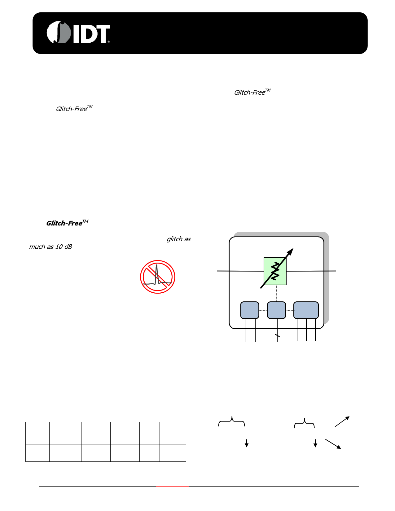
GENERAL DESCRIPTION
This document describes the specification for the
IDTF1950 Digital Step Attenuator. The F1950 is part of a
family of Glitch-FreeTM DSAs optimized for the demanding
requirements of communications Infrastructure. These
devices are offered in a compact 4x4 QFN package with
50 Ω impedances for ease of integration into the radio
system.
COMPETITIVE ADVANTAGE
Digital step attenuators are used in Receivers and
Transmitters to provide gain control. The IDTF1950 is a
7-bit step attenuator optimized for these demanding
applications. The silicon design has very low insertion
loss and low distortion (+65 dBm IP3I.) The device has
pinpoint accuracy and settles to final attenuation value
within 400 nsec. Most importantly, the F1950 includes
IDT’s Glitch-FreeTM technology which results in less
than 0.6 dB of overshoot ringing during MSB transitions.
This is in stark contrast to competing DSAs that glitch as
much as 10 dB during MSB transitions (see p.10)
Lowest insertion loss for best SNR
Glitch-FreeTM when transitioning –
won’t damage PA or ADC
Extremely accurate with low distortion
Glitch-FreeTTMM
APPLICATIONS
• Base Station 2G, 3G, 4G, TDD radiocards
• Repeaters and E911 systems
• Digital Pre-Distortion
• Point to Point Infrastructure
• Public Safety Infrastructure
• WIMAX Receivers and Transmitters
• Military Systems, JTRS radios
• RFID handheld and portable readers
• Cable Infrastructure
PART# MATRIX
Part#
F1950
F1951
F1952
Freq range
150 - 4000
100 - 4000
100 – 4000
Resolution
/ Range
0.25 / 31.75
0.50 / 31.5
0.50 / 15.5
Control
Parallel &
Serial
Serial Only
Serial Only
IL
-1.3
-1.2
-0.9
Pinout
PE
HITT
HITT
IDTF1950
DATASHEET
150 MHz to 4000 MHz
FEATURES
• Glitch-FreeTM, < 0.6 dB transient overshoot
• Spurious Free Design
• 3V to 5V supply
• Attenuation Error < 0.3 dB @ 2 GHz
• Low Insertion Loss < 1.3 dB @ 2 GHz
• Excellent Linearity +65 dBm IP3I
• Fast settling time, < 400 nsec
• Class 2 JEDEC ESD (> 2kV HBM)
• Serial & Parallel Interface 31.75 dB Range
• 4x4 mm Thin QFN 24 pin package
DEVICE BLOCK DIAGRAM
RF1 RF2
Bias
DEC
SPI
VMODE VDD
7
D[6:0] CLK DATA LE
ORDERING INFORMATION
Omit IDT
prefix
0.8 mm height
package
Tape &
Reel
IDTF1950NBGI8
RF product Line
Green
Industrial
Temp range
Glitch-FreeTM Digital Step Attenuator
1
Rev1 March 2012
1 page 
IDTF1950
DATASHEET
7-bit 0.25 dB Digital Step Attenuator
150 MHz to 4000 MHz
PARALLEL CONTROL MODE
The user has the option of running in one of two parallel modes: Direct Parallel Mode or Latched Parallel
Mode.
DIRECT PARALLEL MODE:
Direct Parallel Mode is selected when VMODE (pin 3) is < VIL and LE (pin 16) is > VIH. In this mode the
device will immediately react to any voltage changes to the parallel control pins [pins 19, 20, 21, 22, 23,
24, 1]. Use direct parallel mode for the fastest settling time.
LATCHED PARALLEL MODE:
Latched Parallel Mode is selected when VMODE (pin 3) is < VIL and LE (pin 16) is toggled from < VIL to > VIH
To utilize Latched Parallel Mode:
Set LE < VIL
Adjust pins [19, 20, 21, 22, 23, 24, 1] to the desired attenuation setting. (Note the device will not
react to these pins while LE < VIL.)
Pull LE > VIH. The device will then transition to the attenuation settings reflected by these pins.
Latched Parallel Mode implies a default state for when the device is powered up with VMODE < VIL and LE < VIL.
In this case the default setting is MAXIMUM Attenuation.
LATCHED PARALLEL MODE TIMING DIAGRAM: (Note the Timing Spec Intervals in Blue)
VMODE
Spec
Intervals
LE
A
C
DB
Data Word
Latched into
Active Register
D[6:0]
LATCHED PARALLEL MODE TIMING TABLE:
Interval
Symbol
A
B
C
D
Description
Serial to Parallel Mode Setup Time
Parallel Data Hold Time
LE minimum pulse width
Parallel Data Setup Time
Glitch-FreeTM Digital Step Attenuator
5
Min
Spec
100
10
10
10
Max
Spec
Units
nsec
nsec
nsec
nsec
Rev1 March 2012
5 Page 
7-bit 0.25 dB Digital Step Attenuator
PIN DIAGRAM (F1950)
IDTF1950
DATASHEET
150 MHz to 4000 MHz
24 23 22 21 20 19
D0 1
VDD
2
VMODE
3
GND 4
*RF1 5
GND 6
Exposed Pad
Package Drawing
4 mm x 4 mm package dimension
2.60 mm x 2.60 mm exposed pad
0.5 mm pitch
24 pins
0.75 mm height
0.25 mm pad width
0.40 mm pad length
18 DATA
17 CLK
16 LE
15 GND
14 *RF2
13 GND
7 8 9 10 11 12
* Device is RF Bi-Directional
Glitch-FreeTM Digital Step Attenuator
11
Rev1 March 2012
11 Page | ||
| Páginas | Total 17 Páginas | |
| PDF Descargar | [ Datasheet IDTF1950.PDF ] | |
Hoja de datos destacado
| Número de pieza | Descripción | Fabricantes |
| IDTF1950 | 7-bit 0.25 dB Digital Step Attenuator | Integrated Device Technology |
| IDTF1951 | 6-bit 0.5 dB Digital Step Attenuator | Integrated Device Technology |
| Número de pieza | Descripción | Fabricantes |
| SLA6805M | High Voltage 3 phase Motor Driver IC. |
Sanken |
| SDC1742 | 12- and 14-Bit Hybrid Synchro / Resolver-to-Digital Converters. |
Analog Devices |
|
DataSheet.es es una pagina web que funciona como un repositorio de manuales o hoja de datos de muchos de los productos más populares, |
| DataSheet.es | 2020 | Privacy Policy | Contacto | Buscar |