|
|
PDF NCP81166 Data sheet ( Hoja de datos )
| Número de pieza | NCP81166 | |
| Descripción | Synchronous Buck MOSFET Drivers | |
| Fabricantes | ON Semiconductor | |
| Logotipo | ||
Hay una vista previa y un enlace de descarga de NCP81166 (archivo pdf) en la parte inferior de esta página. Total 9 Páginas | ||
|
No Preview Available !
NCP81166, NCP81166A
Synchronous Buck MOSFET
Drivers
The NCP81166/A is a high performance dual MOSFET gate driver
optimized to drive the gates of both high−side and low−side power
MOSFETs in a synchronous buck converter. 2mm x 2mm DFN8
package allows for space−optimized board layout.
Zero current detect feature allows for a high−efficiency solution
even at light load conditions. Pre−OVP feature aids in protecting the
load in the event of a short across the high−side FET. VCC UVLO
ensures the MOSFETs are off when supply voltages are low. A
bi−directional Enable pin provides a fault signal to the controller
when a pre−OVP or UVLO fault is detected.
http://onsemi.com
1
DFN8
MN SUFFIX
CASE 506CN
Features
• Space−Efficient 2 mm x 2mm DFN8 Thermally−Enhanced Package
• VCC Range of 4.5 V to 13.2 V
• Integrated Bootstrap Diode
• Pre−OVP Function Protects Load during HS FET Short
♦ NCP81166: 2.25 V SW Trip Threshold
♦ NCP81166A: 1.8 V SW Trip Threshold
• Zero Current Detect Function Provides Power Saving Operation
during Light Load Conditions
• Bi−directional Enable Feature pulls Enable pin low during pre−OVP
and UVLO Faults
• 5 V tri−state PWM Logic
• Adaptive Anti−Cross−Conduction Circuit Protects against
Cross−Conduction during FET turn−on and turn−off
• Output Disable Control turns off both MOSFETs via Enable pin
• VCC Undervoltage Lockout
• Direct interface to ASP1252, ASP1400 and other compatible PWM
Controllers
• These Devices are Pb−Free, Halogen Free/BFR Free and are RoHS
Compliant
Typical Applications
• Power Solutions for Desktop Systems
MARKING DIAGRAM
1
XXMG
G
XX = Specific Device Code
CE for NCP81166
CH for NCP81166A
M = Date Code
G = Pb−Free Device
(Note: Microdot may be in either location)
ORDERING INFORMATION
Device
Package
Shipping†
NCP81166MNTBG
DFN8
3000 / Tape &
(Pb−Free)
Reel
NCP81166AMNTBG DFN8
3000 / Tape &
(Pb−Free)
Reel
†For information on tape and reel specifications,
including part orientation and tape sizes, please
refer to our Tape and Reel Packaging Specification
Brochure, BRD8011/D.
© Semiconductor Components Industries, LLC, 2015
January, 2015 − Rev. 2
1
Publication Order Number:
NCP81166/D
1 page 
NCP81166, NCP81166A
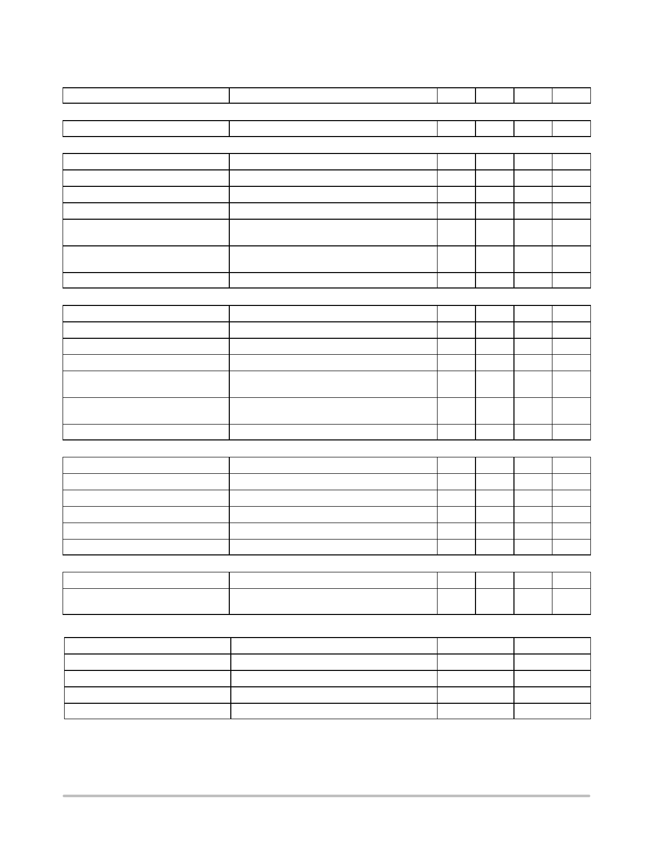
Table 4. ELECTRICAL CHARACTERISTICS (Unless otherwise stated: −10°C < TA < +125°C; 4.5 V < VCC < 13.2 V,
4.5 V < BST−SWN < 13.2 V, 4.5 V < BST < 30 V, 0 V < SWN < 21 V)
Parameter
Test Conditions
Min. Typ. Max.
HIGH SIDE DRIVER (VCC = 5 V)
DRVH Pull Down Resistance
DRVH to SW, BST−SW = 0 V
45
LOW SIDE DRIVER (VCC = 12 V)
Output Impedance, Sourcing Current
2.0 3.0
Output Impedance, Sinking Current
0.7 1.5
DRVL Rise Time trDRVL
DRVL Fall Time tfDRVL
DRVL Turn−Off Propagation Delay
tpdlDRVL
CLOAD = 3 nF
CLOAD = 3 nF
CLOAD = 3 nF
16 35
11 20
35
DRVL Turn−On Propagation Delay
tpdhDRVL
CLOAD = 3 nF
8.0 30
DRVL Pull Down Resistance
DRVL to PGND, VCC = PGND
45
LOW SIDE DRIVER (VCC = 5 V)
Output Impedance, Sourcing Current
2.5
Output Impedance, Sinking Current
1.0
DRVL Rise Time trDRVL
DRVL Fall Time tfDRVL
DRVL Turn−Off Propagation Delay
tpdlDRVL
CLOAD = 3 nF
CLOAD = 3 nF
CLOAD = 3 nF
30
22
27
DRVL Turn−On Propagation Delay
tpdhDRVL
CLOAD = 3 nF
12
DRVL Pull Down Resistance
DRVL to PGND, VCC = PGND
45
EN INPUT
Input Voltage High
2.0
Input Voltage Low
1.0
Hysteresis
500
Normal Mode Bias Current
−1 1
Enable Pin Sink Current
4 30
Propagation Delay Time
20 40
SW Node
SW Node Leakage Current
20
Zero Cross Detection Threshold Voltage SW to −20 mV, ramp slowly until BG goes off
(Start in DCM mode) (Note 3)
−6
Units
kW
W
W
ns
ns
ns
ns
kW
W
W
ns
ns
ns
ns
kW
V
V
mV
mA
mA
ns
mA
mV
Table 5. DECODER TRUTH TABLE
PWM INPUT
PWM High
PWM Mid
PWM Mid
PWM Low
3. Guaranteed by design; not production tested.
ZCD
ZCD Reset
Positive current through the inductor
Zero current through the inductor
ZCD Reset
DRVL
Low
High
Low
High
DRVH
High
Low
Low
Low
http://onsemi.com
5
5 Page | ||
| Páginas | Total 9 Páginas | |
| PDF Descargar | [ Datasheet NCP81166.PDF ] | |
Hoja de datos destacado
| Número de pieza | Descripción | Fabricantes |
| NCP81161 | VR12.5 Compatible Synchronous Buck MOSFET Drivers | ON Semiconductor |
| NCP81166 | Synchronous Buck MOSFET Drivers | ON Semiconductor |
| NCP81166A | Synchronous Buck MOSFET Drivers | ON Semiconductor |
| Número de pieza | Descripción | Fabricantes |
| SLA6805M | High Voltage 3 phase Motor Driver IC. |
Sanken |
| SDC1742 | 12- and 14-Bit Hybrid Synchro / Resolver-to-Digital Converters. |
Analog Devices |
|
DataSheet.es es una pagina web que funciona como un repositorio de manuales o hoja de datos de muchos de los productos más populares, |
| DataSheet.es | 2020 | Privacy Policy | Contacto | Buscar |
