|
|
|
PDF NCP4305 Data sheet ( Hoja de datos )
| Número de pieza | NCP4305 | |
| Descripción | Secondary Side Synchronous Rectification Driver | |
| Fabricantes | ON Semiconductor | |
| Logotipo | ||
Hay una vista previa y un enlace de descarga de NCP4305 (archivo pdf) en la parte inferior de esta página. Total 30 Páginas | ||
|
No Preview Available !
NCP4305
Secondary Side
Synchronous Rectification
Driver for High Efficiency
SMPS Topologies
The NCP4305 is high performance driver tailored to control a
www.onsemi.com
synchronous rectification MOSFET in switch mode power supplies.
Thanks to its high performance drivers and versatility, it can be used in
MARKING
DIAGRAMS
various topologies such as DCM or CCM flyback, quasi resonant
flyback, forward and half bridge resonant LLC.
The combination of externally adjustable minimum off-time and
on-time blanking periods helps to fight the ringing induced by the PCB
layout and other parasitic elements. A reliable and noise less operation
of the SR system is insured due to the Self Synchronization feature. The
8
1
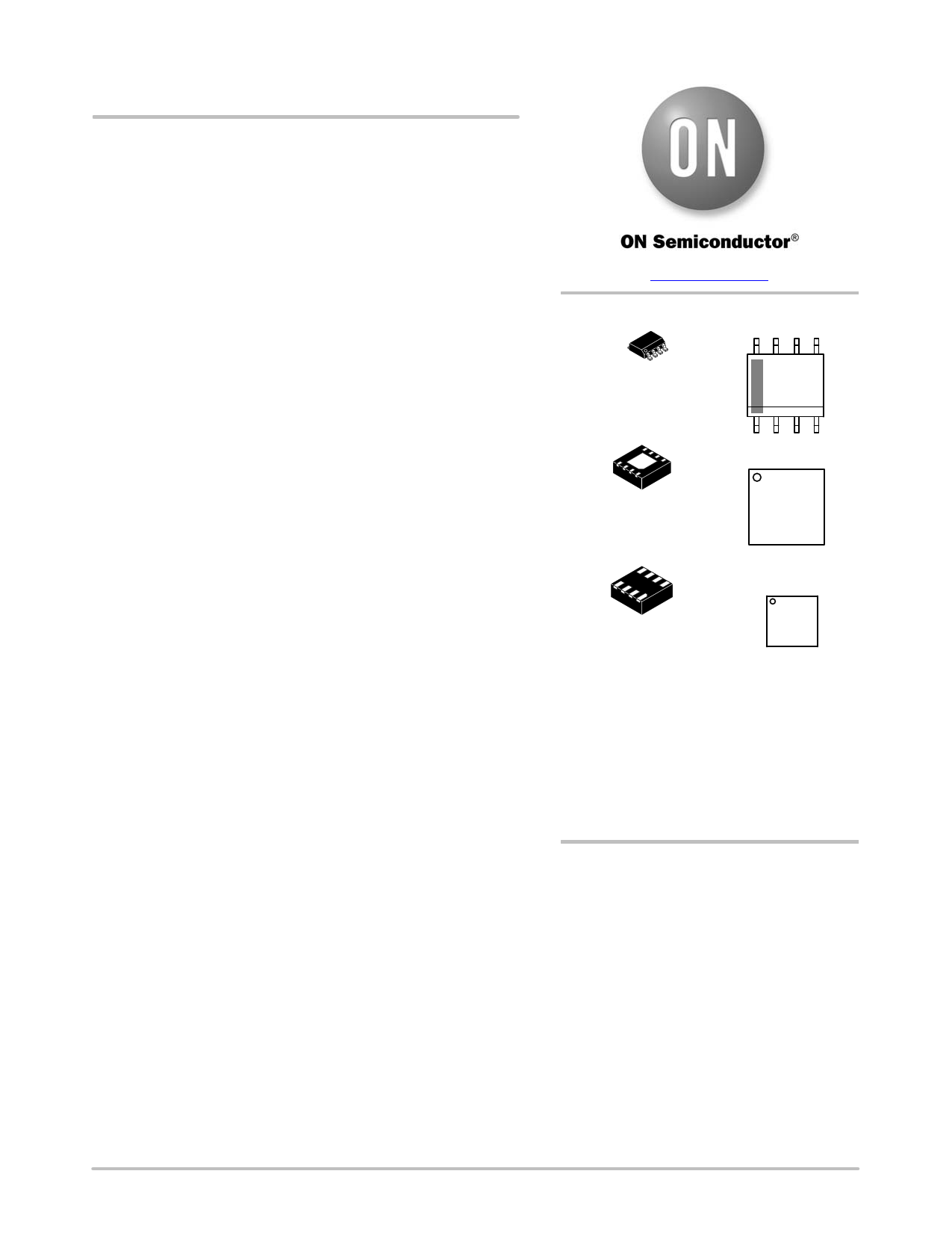
SOIC−8
D SUFFIX
CASE 751
8
NCP4305x
ALYW G
G
1
NCP4305 also utilizes Kelvin connection of the driver to the MOSFET
to achieve high efficiency operation at full load and utilizes a light load
detection architecture to achieve high efficiency at light load.
1 4305x
The precise turn−off threshold, extremely low turn−off delay time
and high sink current capability of the driver allow the maximum
synchronous rectification MOSFET conduction time and enables
DFN8
MN SUFFIX
CASE 488AF
ALYWG
G
maximum SMPS efficiency. The high accuracy driver and 5 V gate
clamp enables the use of GaN FETs.
Features
• Self−Contained Control of Synchronous Rectifier in CCM, DCM and
QR for Flyback, Forward or LLC Applications
• Precise True Secondary Zero Current Detection
• Typically 12 ns Turn off Delay from Current Sense Input to Driver
• Rugged Current Sense Pin (up to 200 V)
WDFN8
MT SUFFIX
CASE 511AT
1
5xMG
G
4305x = Specific Device Code
x = A, B, C, D or Q
A = Assembly Location
• Ultrafast Turn−off Trigger Interface/Disable Input (7.5 ns)
• Adjustable Minimum ON−Time
• Adjustable Minimum OFF-Time with Ringing Detection
• Adjustable Maximum ON−Time for CCM Controlling of Primary
QR Controller
L = Wafer Lot
Y = Year
W = Work Week
M = Date Code
G = Pb−Free Package
(Note: Microdot may be in either location)
• Improved Robust Self Synchronization Capability
• 8 A / 4 A Peak Current Sink / Source Drive Capability
• Operating Voltage Range up to VCC = 35 V
• Automatic Light−load & Disable Mode
ORDERING INFORMATION
See detailed ordering and shipping information on page 49 of
this data sheet.
• Adaptive Gate Drive Clamp
• GaN Transistor Driving Capability (options A and C)
• Low Startup and Disable Current Consumption
• Maximum Operation Frequency up to 1 MHz
• SOIC-8 and DFN−8 (4x4) and WDFN8 (2x2) Packages
• These are Pb−Free Devices
Typical Applications
• Notebook Adapters
• High Power Density AC/DC Power Supplies (Cell
Phone Chargers)
• LCD TVs
• All SMPS with High Efficiency Requirements
© Semiconductor Components Industries, LLC, 2015
June, 2015 − Rev. 1
1
Publication Order Number:
NCP4305/D
1 page 
NCP4305
MIN_TON
CS
ELAPSED
ADJ Minimum ON time
generator
EN
VDD
100mA
CS_ON
CS
detection
CS_OFF
CS_RESET
MIN_TOFF
RESET
ADJ Minimum OFF ELAPSED
time generator EN
MAX_TON
ELAPSED
ADJ Maximum ON time
generator
EN
DISABLE
Disable detection
&
V DRV clamp
modulation
V_DRV
control
LLD
Control logic
DRIVER
DRV Out
DRV
VDD
VCC managment
DISABLE
UVLO
VCC
GND
Figure 6. Internal Circuit Architecture − NCP4305Q (CCM QR) with MAX_TON
www.onsemi.com
5
5 Page 
NCP4305
0.80
0.75
0.70
0.65
0.60
0.55
0.50
0.45
0.40
0.35
0.30
0
TYPICAL CHARACTERISTICS
5 10 15 20 25 30
VCC (V)
Figure 21. CS Reset Threshold
35
200
180
160
140
120
100
80
60
40
20
0
−40 −20 0 20 40 60 80 100
TJ (°C)
Figure 22. CS Leakage, VCS = 200 V
120
60
55
50
45
40
35
30
25
20
−40 −20 0 20 40 60 80 100 120
TJ (°C)
Figure 23. Propagation Delay from CS to DRV
Output On
2.15
2.13
2.11
2.09
2.07
2.05
2.03
2.01
1.99
1.97
1.95
−40 −20 0 20 40 60 80 100 120
TJ (°C)
Figure 25. Trigger Threshold, VCC = 12 V
24
22
20
18
16
14
12
10
8
6
4
−40 −20 0 20 40 60 80 100 120
TJ (°C)
Figure 24. Propagation Delay from CS to DRV
Output Off
2.5
2.4
2.3
2.2
2.1
2.0
1.9
1.8
1.7
1.6
1.5
0
TJ = 125°C
TJ = 85°C
TJ = 55°C
TJ = 25°C
TJ = 0°C
TJ = −20°C
TJ = −40°C
5 10 15 20 25 30
VCC (V)
Figure 26. Trigger Threshold
35
www.onsemi.com
11
11 Page | ||
| Páginas | Total 30 Páginas | |
| PDF Descargar | [ Datasheet NCP4305.PDF ] | |
Hoja de datos destacado
| Número de pieza | Descripción | Fabricantes |
| NCP4300A | Dual Operational Amplifier and Voltage Reference | ON |
| NCP4300ADR2 | Dual Operational Amplifier and Voltage Reference | ON |
| NCP4302 | Synchronous Rectification Controller | ON Semiconductor |
| NCP4303A | Secondary Side Synchronous Rectification Driver | ON Semiconductor |
| Número de pieza | Descripción | Fabricantes |
| SLA6805M | High Voltage 3 phase Motor Driver IC. |
Sanken |
| SDC1742 | 12- and 14-Bit Hybrid Synchro / Resolver-to-Digital Converters. |
Analog Devices |
|
DataSheet.es es una pagina web que funciona como un repositorio de manuales o hoja de datos de muchos de los productos más populares, |
| DataSheet.es | 2020 | Privacy Policy | Contacto | Buscar |