|
|
|
PDF NCP383 Data sheet ( Hoja de datos )
| Número de pieza | NCP383 | |
| Descripción | Adjustable Current-Limiting Power-Distribution Switches | |
| Fabricantes | ON Semiconductor | |
| Logotipo | ||
Hay una vista previa y un enlace de descarga de NCP383 (archivo pdf) en la parte inferior de esta página. Total 10 Páginas | ||
|
No Preview Available !
NCP383
Adjustable Current-Limiting
Power-Distribution
Switches
The NCP383 is a single input dual outputs power−distribution
switch designed for applications where heavy capacitive loads and
short−circuits are likely to be encountered, incorporating two very low
RDS(on), N−channel MOSFETs in a single package. Each channel of
the device limits the output current to a desired level by switching into
a constant−current mode when the output load exceeds the
current−limit threshold or a short circuit is present. The current−limit
threshold is externally fixed by a pull down resistor placed between
Ilim and GND. The power−switches rise and fall times are controlled to
minimize current ringing during turn on/off.
An internal reverse−voltage detection comparator disables the
power−switch if the output voltage is higher than the input voltage to
protect devices on the input side of the switches.
The /FLAGx logic output asserts low during over−current,
reverse−voltage or over temperature conditions. The switch is
controlled by a logic enable input active low.
Features
• 2.7 V – 5.5 V Operating Range
• Current limit: Adjustable up to 2.8 A
• ± 7.5% Current Limit Accuracy at 2.8 A
• Very fast Over−Current Detection Response: 2 ms (typ)
• 1 mA Maximum Standby Supply Current
• Under Voltage Lock−out (UVLO)
• Soft−Start Prevents Inrush Current
• Thermal Protection
• Soft Turn−off
• Reverse Voltage Protection
• Enable Active Low
• mDFN 3x3 mm
• Compliance to IEC61000−4−2 (Level 4)
8.0 kV (Contact) − 15 kV (Air)
• UL Listed – File E343275
• CB − IEC60950−ED2 Certified
• CB – IEC60950−ED2−AM1 Certified
• This is a Pb−Free Device
Typical Applications
• Laptops
• USB Ports/Hubs
• TVs
http://onsemi.com
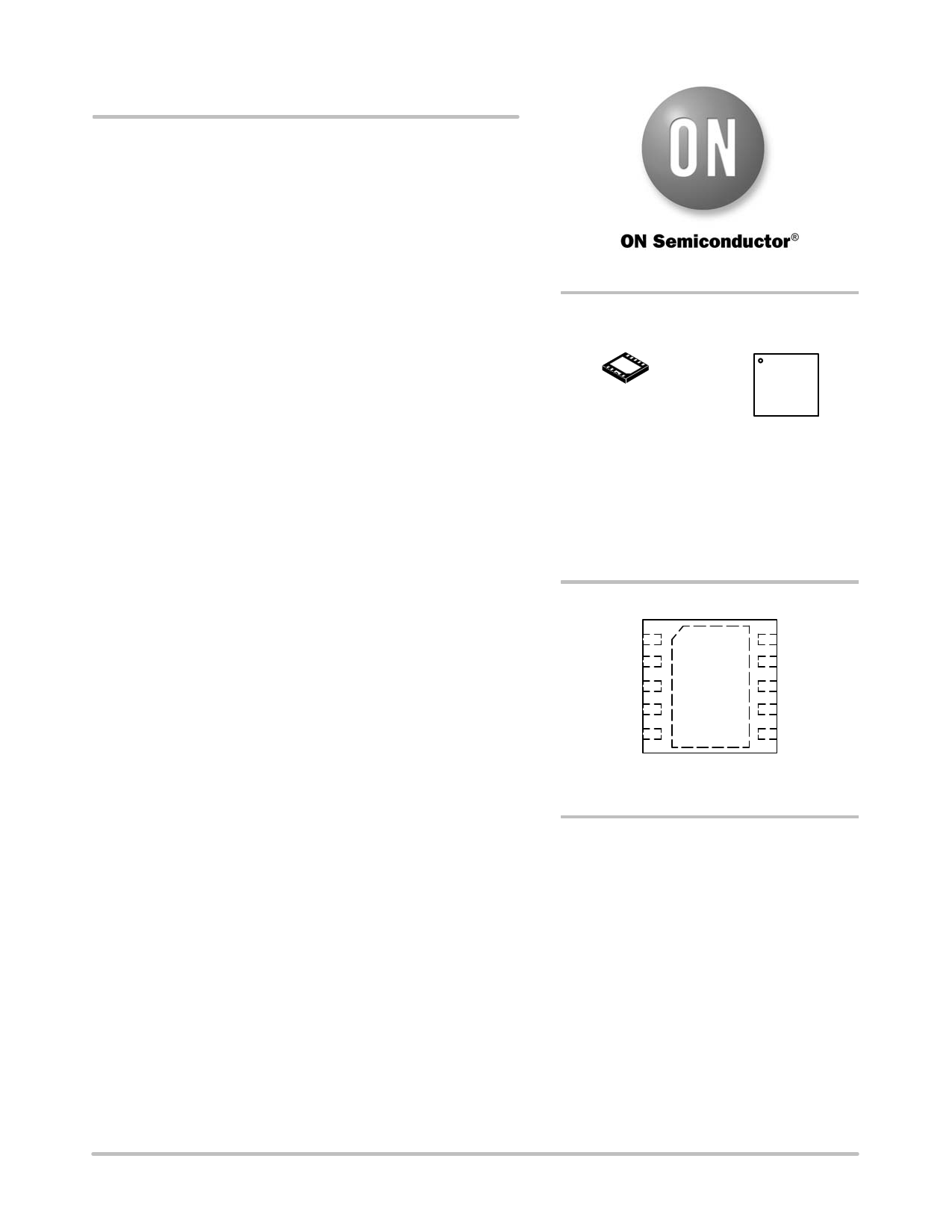
UDFN10
CASE 517CC
MARKING
DIAGRAM
383
ALYWG
G
A = Assembly Location
L = Wafer Lot
Y = Year
W = Work Week
G = Pb−Free Package
(*Note: Microdot may be in either location)
PIN CONNECTIONS
GND 1
IN 2
IN 3
EN1 4
EN2 5
10 /FLAG1
9 OUT1
8 OUT2
7 ILIM
6 /FLAG2
(Top View)
Exposed pad must be soldered to PCB Ground plane.
ORDERING INFORMATION
See detailed ordering and shipping information in the package
dimensions section on page 9 of this data sheet.
© Semiconductor Components Industries, LLC, 2012
October, 2012 − Rev. 2
1
Publication Order Number:
NCP383/D
1 page 
NCP383
ELECTRICAL CHARACTERISTICS Min & Max Limits apply for TA between −40°C to +85°C and TJ up to + 125°C for VIN between
2.5 V to 5.5 V (Unless otherwise noted). Typical values are referenced to TA = + 25°C and VIN = 5 V.
Symbol
Parameter
Conditions
Conditions
Min Typ Max Unit
POWER SWITCH
RDS(on)
TR
TF
Static drain−source on−state
resistance, per channel
Output rise time
Output fall time
TJ = 25°C
–40°C < TJ < 125°C
VIN = 5 V
VIN = 5 V
CLOAD = 1mF,
RLOAD = 100 W
(Note 9)
45 70
95 mW
1.5 2.5
4
ms
0.1 0.5
Logic Pins
VIHEN
High−level input voltage
VILEN
Low−level input voltage
IENx Input current
TON Turn on time
TOFF
Turn off time
CURRENT LIMIT
VENx = 0 V, V/ENx = 5 V
CLOAD = 1mF, RLOAD = 100 W (Note 9)
1.2
−0.5
1
1
−
V
0.4 V
0.5 mA
9 ms
3 ms
IOCP
Current−limit threshold (Max-
imum DC output current
IOUTX delivered to load)
Ilimx = 90k (Note 10)
Ilimx = 56k
Ilimx = 20k (Note 10)
0.5 0.6 0.7
0.9 1 1.1
2.58 2.8 3.01
A
TDET
Response time to short circuit
TREG
Regulation time
TOCP
Over current protection time
UNDERVOLTAGE LOCKOUT
VIN = 5 V (Note 10)
2 ms
1 2 3 ms
19 24 29 ms
VUVLO
IN pin low−level input voltage
VHYST
IN pin hysteresis
TRUVLO
Re−arming Time
SUPPLY CURRENT
VIN rising
TJ = 25°C
− 2.45 2.5
V
25 mV
7 12 15 ms
IINOFF
IINON
Low−level output supply cur-
rent.
High−level output supply cur-
rent.
IREV Reverse leakage current
/FLAGx PINS
VIN = 5 V, No load on OUTX, Device OFF
VENX= 0 V or V/ENX= 5 V – TJ = 25°C
VIN = 5 V, No load on OUTX
Device ON − RILIM = 56 kW − VENX= 5 V
VOUTX = 5 V,
VIN = 0 V
TJ = 25°C
1 mA
99 mA
1 mA
VOL /FLAGX output low voltage
ILEAK
Off−state leakage
TFGL
/FLAGX deglitch
TFOCP
/FLAGX deglitch
TFREV
/FLAGX deglitch
REVERSE VOLTAGE PROTECTION
I/FLAGX = 1 mA
V/FLAGX = 5 V
/FLAGX de−assertion time due to overcurrent
/FLAGX assertion due to overcurrent
/FLAGX assertion due to reverse−voltage
3
5
3
400 mV
1 mA
5 7 ms
7 12 ms
5 7 ms
VREV
VRHYST
Reverse voltage threshold
Reverse voltage threshold
hysteresis
VOUT − VIN drop
VOUT − VIN drop decrease
150 mV
30 mV
THERMAL SHUTDOWN
TSD
TSDOCP
TRST
Thermal shutdown threshold
Thermal regulation threshold
Thermal regulation rearming
threshold
140 °C
125 °C
115 °C
9. Parameters are guaranteed for CLOAD and RLOAD connected to the OUT pin with respect to the ground.
10. Guaranteed by design and by characterization
http://onsemi.com
5
5 Page | ||
| Páginas | Total 10 Páginas | |
| PDF Descargar | [ Datasheet NCP383.PDF ] | |
Hoja de datos destacado
| Número de pieza | Descripción | Fabricantes |
| NCP380 | Fixed/Adjustable Current Limiting Power DistributionSwitches | ON Semiconductor |
| NCP3800V | SMBus Level 2 Battery Charger | ON Semiconductor |
| NCP383 | Adjustable Current-Limiting Power-Distribution Switches | ON Semiconductor |
| Número de pieza | Descripción | Fabricantes |
| SLA6805M | High Voltage 3 phase Motor Driver IC. |
Sanken |
| SDC1742 | 12- and 14-Bit Hybrid Synchro / Resolver-to-Digital Converters. |
Analog Devices |
|
DataSheet.es es una pagina web que funciona como un repositorio de manuales o hoja de datos de muchos de los productos más populares, |
| DataSheet.es | 2020 | Privacy Policy | Contacto | Buscar |