|
|
|
PDF LE25U40PCMC Data sheet ( Hoja de datos )
| Número de pieza | LE25U40PCMC | |
| Descripción | 4M-bit (512K x 8) Serial Flash Memory | |
| Fabricantes | ON Semiconductor | |
| Logotipo | ||
Hay una vista previa y un enlace de descarga de LE25U40PCMC (archivo pdf) en la parte inferior de esta página. Total 23 Páginas | ||
|
No Preview Available !
LE25U40PCMC
Advance Information
CMOS LSI
4M-bit (512K x 8)
Serial Flash Memory
www.onsemi.com
Overview
The LE25U40PCMC is a SPI bus flash memory device with a 4M bit (512K
8-bit) configuration that adds a high performance Dual output and Dual I/O
function. It uses a single 2.5V power supply. While making the most of the
features inherent to a serial flash memory device, the LE25U40PCMC is
housed in an 8-pin ultra-miniature package. All these features make this device
ideally suited to storing program in applications such as portable information
devices, which are required to have increasingly more compact dimensions.
The LE25U40PCMC also has a small sector erase capability which makes the
device ideal for storing parameters or data that have fewer rewrite cycles and
conventional EEPROMs cannot handle due to insufficient capacity.
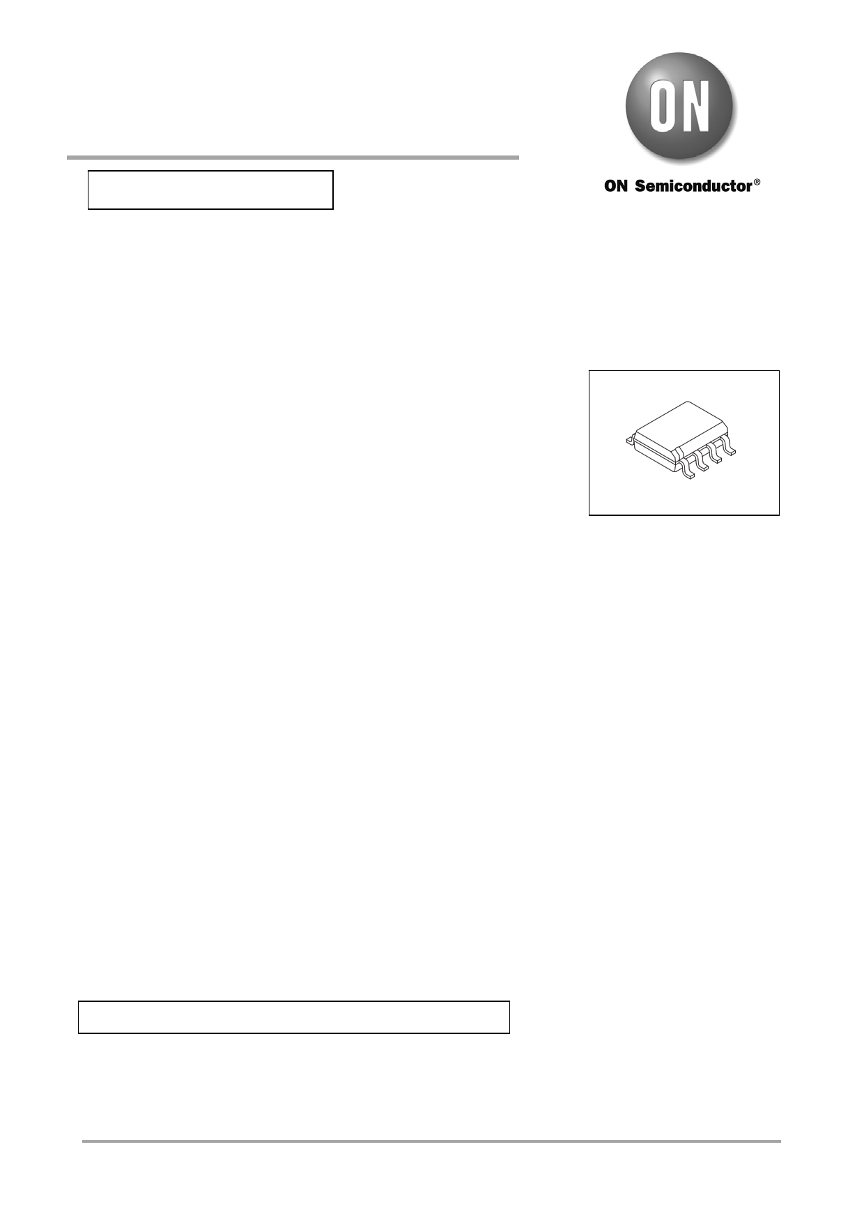
SOIC-8 / SOP8J (200mil)
Features
Read/write operations enabled by single 2.5V power supply: 2.3 to 3.6V supply voltage range
Operating frequency : 30MHz
Temperature range
: 40 to 105C
Serial interface
: SPI mode 0, mode 3 supported / Dual Output, Dual I/O supported
Sector size
: 4K bytes/small sector, 64K bytes/sector
Small sector erase, sector erase, chip erase functions
Page program function (256 bytes / page)
Block protect function
Highly reliable read/write
Number of rewrite times : 100,000 times
Small sector erase time : 40ms (typ.), 150ms (max.)
Sector erase time
: 80ms (typ.), 250ms (max.)
Chip erase time
: 250ms (typ.), 2.0s (max.)
Page program time : 4.0ms/256 bytes (typ.), 5.0ms/256 bytes (max.)
Status functions
: Ready/busy information, protect information
Data retention period : 20 years
Package
: SOP8J (200mil), CASE 751CU
* This product is licensed from Silicon Storage Technology, Inc. (USA).
This document contains information on a new product. Specifications and information
herein are subject to change without notice.
ORDERING INFORMATION
See detailed ordering and shipping information on page 23 of this data sheet.
© Semiconductor Components Industries, LLC, 2015
January 2015 - Rev. P0
1
Publication Order Number :
LE25U40PCMC/D
1 page 
Table 3 Command Settings
4M Bit
sector(64KB)
7
6
5
4
3
2
1
0
LE25U40PCMC
small sector
127
to
112
111
to
96
95
to
80
79
to
64
63
to
48
47
to
32
31
to
16
15
to
2
1
0
address space(A23 to A0)
07F000h
07FFFFh
070000h
06F000h
070FFFh
06FFFFh
060000h
05F000h
060FFFh
05FFFFh
050000h
04F000h
050FFFh
04FFFFh
040000h
03F000h
040FFFh
03FFFFh
030000h
02F000h
030FFFh
02FFFFh
020000h
01F000h
020FFFh
01FFFFh
010000h
00F000h
010FFFh
00FFFFh
002000h
001000h
000000h
002FFFh
001FFFh
000FFFh
www.onsemi.com
5
5 Page 
LE25U40PCMC
4. Write Enable
Before performing any of the operations listed below, the device must be placed in the write enable state. Operation is
the same as for setting status register WEN to "1", and the state is enabled by inputting the write enable command.
"Figure 8 Write Enable" shows the timing waveforms when the write enable operation is performed. The write enable
command consists only of the first bus cycle, and it is initiated by inputting (06h).
Small sector erase, sector erase, chip erase
Page program
Status register write
5. Write Disable
The write disable command sets status register WEN to "0" to prohibit unintentional writing. "Figure 9 Write Disable"
shows the timing waveforms. The write disable command consists only of the first bus cycle, and it is initiated by
inputting (04h). The write disable state (WEN "0") is exited by setting WEN to "1" using the write enable command
(06h).
Figure 8 Write Enable
Figure 9 Write Disable
CS CS
SCK
SI
SO
Mode3
Mode0
01234567
8CLK
06h
MSB
High Impedance
SCK
SI
SO
Mode3
Mode0
01234567
8CLK
MSB
04h
High Impedance
6. Power-down
The power-down command sets all the commands, with the exception of the silicon ID read command and the
command to exit from power-down, to the acceptance prohibited state (power-down). "Figure 10 Power-down" shows
the timing waveforms. The power-down command consists only of the first bus cycle, and it is initiated by inputting
(B9h). However, a power-down command issued during an internal write operation will be ignored. The power-down
state is exited using the power-down exit command (power-down is exited also when one bus cycle or more of the
silicon ID read command (ABh) has been input). "Figure 11 Exiting from Power-down" shows the timing waveforms
of the power-down exit command.
CS
SCK
SI
SO
Figure 10 Power-down
Power down
mode
Mode3
Mode0
01234567
tDP
8CLK
MSB
B9h
High Impedance
CS
SCK
SI
SO
Figure 11 Exiting from Power-down
Power down
mode
Mode3
Mode0
01234567
tPDR
8CLK
MSB
ABh
High Impedance
www.onsemi.com
11
11 Page | ||
| Páginas | Total 23 Páginas | |
| PDF Descargar | [ Datasheet LE25U40PCMC.PDF ] | |
Hoja de datos destacado
| Número de pieza | Descripción | Fabricantes |
| LE25U40PCMC | 4M-bit (512K x 8) Serial Flash Memory | ON Semiconductor |
| Número de pieza | Descripción | Fabricantes |
| SLA6805M | High Voltage 3 phase Motor Driver IC. |
Sanken |
| SDC1742 | 12- and 14-Bit Hybrid Synchro / Resolver-to-Digital Converters. |
Analog Devices |
|
DataSheet.es es una pagina web que funciona como un repositorio de manuales o hoja de datos de muchos de los productos más populares, |
| DataSheet.es | 2020 | Privacy Policy | Contacto | Buscar |