|
|
|
PDF NCP5220A Data sheet ( Hoja de datos )
| Número de pieza | NCP5220A | |
| Descripción | 3-in-1 PWM Dual Buck and Linear Power Controller | |
| Fabricantes | ON Semiconductor | |
| Logotipo | ||
Hay una vista previa y un enlace de descarga de NCP5220A (archivo pdf) en la parte inferior de esta página. Total 18 Páginas | ||
|
No Preview Available !
NCP5220A
3−in−1 PWM Dual Buck and
Linear Power Controller
The NCP5220A 3−in−1 PWM Dual Buck and Linear Power
Controller, is a complete power solution for MCH and DDR memory.
This IC combines the efficiency of PWM controllers for the VDDQ
supply and the MCH core supply voltage with the simplicity of linear
regulator for the VTT termination voltage.
This IC contains two synchronous PWM buck controllers for
driving four external N−Ch FETs to form the DDR memory supply
voltage (VDDQ) and the MCH regulator. The DDR memory
termination regulator (VTT) is designed to track at half of the
reference voltage with sourcing and sinking current.
Protective features include, soft−start circuitry, undervoltage
monitoring of 5VDUAL, BOOT voltage and thermal shutdown. The
device is housed in a thermal enhanced space−saving DFN−20
package.
Features
• Incorporates Synchronous PWM Buck Controllers for VDDQ and
VMCH
• Integrated Power FETs with VTT Regulator Source/Sink up to 2.0 A
• All External Power MOSFETs are N−Channel
• Adjustable VDDQ and VMCH by External Dividers
• VTT Tracks at Half the Reference Voltage
• Fixed Switching Frequency of 250 kHz for VDDQ and VMCH
• Doubled Switching Frequency of 500 kHz for VDDQ Controller in
Standby Mode to Optimize Inductor Current Ripple and Efficiency
• Soft−Start Protection for All Controllers
• Undervoltage Monitor of Supply Voltages
• Overcurrent Protections for DDQ and VTT Regulators
• VTT Regulators Soft−Start Current Protection
• Fully Complies with ACPI Power Sequencing Specifications
• Short Circuit Protection Prevents Damage to Power Supply Due to
Reverse DIMM Insertion
• Thermal Shutdown
• 5x6 DFN−20 Package
• Pb−Free Package is Available*
Typical Applications
• DDR I and DDR II Memory and MCH Power Supply
*For additional information on our Pb−Free strategy and soldering details, please
download the ON Semiconductor Soldering and Mounting Techniques
Reference Manual, SOLDERRM/D.
http://onsemi.com
20
1
DFN−20
MN SUFFIX
CASE 505AB
MARKING DIAGRAM
N5220A
AWLYYWW G
G
1
N5220A = Device Code
A = Assembly Location
WL = Wafer Lot
YY = Year
WW = Work Week
G = Pb−Free Package
(Note: Microdot may be in either location)
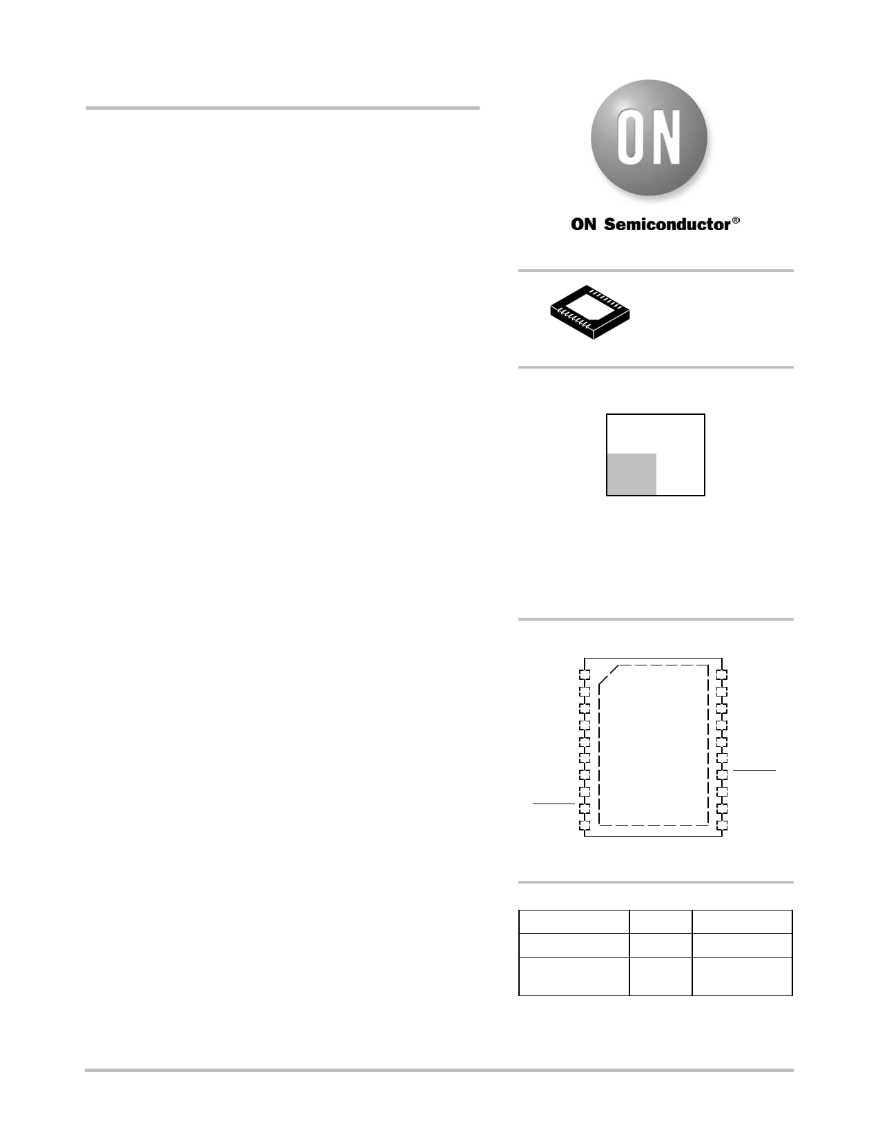
PIN CONNECTIONS
COMP
FBDDQ
SS
PGND
VTT
VDDQ
AGND
FBVTT
SLP_S5
FB1P5
SW_DDQ
BG_DDQ
TG_DDQ
BOOT
5VDUAL
COMP_1P5
SLP_S3
TG_1P5
BG_1P5
GND_1P5
NOTE: Pin 21 is the thermal pad
on the bottom of the device.
ORDERING INFORMATION
Device
Package
Shipping†
NCP5220AMNR2 DFN−20 2500/Tape & Reel
NCP5220AMNR2G DFN−20 2500/Tape & Reel
(Pb−Free)
†For information on tape and reel specifications,
including part orientation and tape sizes, please
refer to our Tape and Reel Packaging Specification
Brochure, BRD8011/D.
© Semiconductor Components Industries, LLC, 2005
December, 2005 − Rev. 4
1
Publication Order Number:
NCP5220A/D
1 page 
NCP5220A
ELECTRICAL CHARACTERISTICS (5VDUAL = 5.0 V, BOOT = 12 V, TA = 0°C to 70°C, L = 1.7 mH, COUT1 = 3770 mF,
COUT2 = 470 mF, COUT3 = NA, CSS = 33 nF, R1 = 2.166 kW, R2 = 2.0 kW, RZ1 = 20 kW, RZ2 = 8.0 W, CP1 = 10 nF,
CZ1 = 6.8 nF, CZ2 = 100 nF, RM1 = 2.166 kW, RM2 = 2.0 kW, RZM1 = 20 kW, RZM2 = 8.0 W, CPM1 = 10 nF, CZM1 = 6.8 nF,
CZM2 = 100 nf for min/max values unless otherwise noted). Duplicate component values of MCH regulator from DDQ.
Characteristic
SUPPLY VOLTAGE
5VDUAL Supplier Rail Voltage
BOOT Supplier Rail Voltage at S0
SUPPLY CURRENT
Symbol
V5VDUAL
VBOOT
Test Conditions
−
−
Min Typ Max
4.5 5.0 5.5
10.5 12 13.2
S0 Mode Supply Current from 5VDUAL
I5VDL_S0
SLP_S5 = HIGH, SLP_S3 = HIGH,
BOOT = 12 V, TG_1P5 and BG_1P5
Open
−
− 10
S3 Mode Supply Current from 5VDUAL
I5VDL_S3 SLP_S5 = HIGH, SLP_S3 = LOW,
TG_1P5 and BG_1P5 Open
−
− 5.0
S5 Mode Supply Current from 5VDUAL
I5VDL_S5
SLP_S5 = LOW, BOOT = 0 V,
TG_1P5 and BG_1P5 Open
− − 1.0
S0 Mode Supply Current from BOOT
IBOOT_S0 SLP_S5 = HIGH, SLP_S3 = HIGH,
BOOT = 12 V, TG_1P5 and BG_1P5
Open
−
− 25
S3 Mode Supply Current from BOOT
IBOOT_S3 SLP_S5 = HIGH, SLP_S3 = LOW,
TG_1P5 and BG_1P5 Open
−
− 25
UNDERVOLTAGE−MONITOR
5VDUAL UVLO Upper Threshold
V5VDLUV+
−
− − 4.4
5VDUAL UVLO Hysteresis
BOOT UVLO Upper Threshold
BOOT UVLO Hysteresis
V5VDLhys
VBOOTUV+
VBOOThys
−
−
−
250 400 550
8.8 − 10.4
− 1.0 1.3
THERMAL SHUTDOWN
Thermal Shutdown
Tsd
(Note 3)
− 145 −
Thermal Shutdown Hysteresis
DDQ SWITCHING REGULATOR
FBDDQ Feedback Voltage, Control Loop in
Regulation
Feedback Input Current
Oscillator Frequency in S0 Mode
Oscillator Frequency in S3 Mode
Oscillator Ramp Amplitude
Tsdhys
VFBQ
IDDQFB
FDDQS0
FDDQS3
dVOSC
(Note 3)
TA = 25°C
TA = 0°C to 70°C
V(FBDDQ) = 1.3 V
−
−
(Note 3)
− 25 −
1.178 1.190 1.202
1.166 − 1.214
− − 1.0
217 250 283
434 500 566
− 1.3 −
Current Limit Blanking Time in S0 Mode
Current Limit Threshold Offset from 5VDUAL
Minimum Duty Cycle
TDDQbk
VOCP
Dmin
(Note 3)
(Note 3)
−
400 −
0.8 −
0−
−
−
−
Maximum Duty Cycle
Dmax
− − − 100
Soft−Start Pin Current for DDQ
DDQ ERROR AMPLIFIER
Iss1
V(SS) = 0 V
3.0 4.0
−
DC Gain
Gain−Bandwidth Product
GAINDDQ
GBWDDQ
(Note 3)
COMP PIN to GND = 220 nF,
1.0 W in Series (Note 3)
− 70 −
− 12 −
Slew Rate
SRDDQ
3. Guaranteed by design, not tested in production.
COMP PIN TO GND = 10 pF
− 8.0 −
Unit
V
V
mA
mA
mA
mA
mA
V
mV
V
V
°C
°C
V
mA
KHz
KHz
Vp−p
nS
V
%
%
mA
dB
MHz
V/uS
http://onsemi.com
5
5 Page 
NCP5220A
For enhanced efficiency, an active synchronous switch is
used to eliminate the conduction loss contributed by the
forward voltage of a diode or Schottky diode rectifier.
Adaptive non−overlap timing control of the complementary
gate drive output signals is provided to reduce
shoot−through current that degrades efficiency.
Tolerance of VDDQ
Both the tolerance of VFBQ and the ratio of the external
resistor divider R1/R2 impact the precision of VDDQ.
With the control loop in regulation, VDDQ = VFBQ ×
(1 + R1/R2). With a worst case (for all valid operating
conditions) VFBQ tolerance of "1.5%, a worst case range
of "2% for VDDQ will be assured if the ratio R1/R2 is
specified as 1.100 "1%.
Fault Protection of VDDQ Regulator
In S0 mode, an internal voltage (VOCP) = 5VDUAL – 0.8
sets the current limit for the high−side switch. The voltage
VOCP pin is compared to the voltage at SWDDQ pin when
the high−side gate drive is turned on after a fixed period of
blanking time to avoid false current limit triggering. When
the voltage at SWDDQ is lower than VOCP, an overcurrent
condition occurs and all regulators are latched off to protect
against overcurrent. The IC will be powered up again if one
of the supply voltages, 5VDUAL, SLP_S5 or 12VATX, is
recycled. The main purpose is for fault protection, not for
precise current limit.
In S3 mode, this overcurrent protection feature is
disabled.
Feedback Compensation of VDDQ Regulator
The compensation network is shown in Figure 2.
VTT Active Terminator
The VTT active terminator is a two quadrant linear
regulator with two internal N−Ch FETs to provide current
sink and source capability up to 2.0 A. It is activated only
when the DDQ regulator is in regulation in S0 mode. It
draws power from VDDQ with the internal gate drive power
derived from 5VDUAL. While VTT output is connecting to
the FBVTT pin directly, VTT voltage is designed to
automatically track at the half of VDDQ. This regulator is
stable with any value of output capacitor greater than
470 mF, and is insensitive to ESR ranging from 1.0 mW to
400 mW.
Fault Protection of VTT Active Terminator
To provide protection for the internal FETs, bi−directional
current limit preset at 2.4 A magnitude is implemented. The
VTT with current limit at 1.0 A provides a soft−start
function during startup in order to avoid overloading at S3
mode.
MCH Switching Regulator
The secondary switching regulator is identical to the DDQ
regulator except the output is 10 A. No fault protection is
implemented and the soft−start timing is twice as fast with
respect to CSS.
BOOT Pin Supply Voltage
In typical application, a flying capacitor is connected
between SWDDQ and BOOT pins. In S0 mode, 12VATX is
tied to BOOT pin through a Schottky diode as well. A 13 V
Zener clamp circuit must clamp this boot strapping voltage
produced by the flying capacitor in S0 mode.
In S3 mode the 12VATX is collapsed and the BOOT
voltage is created by the Schottky diode between 5VDUAL
and BOOT pins as well as the flying capacitor. The
BOOT_UVLO works specially. The _BOOTGD goes low
and the IC remains in S3 mode.
Thermal Consideration
Assuming an ambient temperature of 50°C, the maximum
allowed dissipated power of DFN−20 is 2.8 W, which is
enough to handle the internal power dissipation in S0 mode.
To take full advantage of the thermal capability of this
package, the exposed pad underneath must be soldered
directly onto a PCB metal substrate to allow good
thermal contact.
Thermal Shutdown
When the junction temperature of the IC exceeds 145°C,
the entire IC is shutdown. When the junction temperature
drops below 120°C, the chip resumes normal operation.
http://onsemi.com
11
11 Page | ||
| Páginas | Total 18 Páginas | |
| PDF Descargar | [ Datasheet NCP5220A.PDF ] | |
Hoja de datos destacado
| Número de pieza | Descripción | Fabricantes |
| NCP5220 | PWM Dual Buck and Linear Power Controller | ON Semiconductor |
| NCP5220A | 3-in-1 PWM Dual Buck and Linear Power Controller | ON Semiconductor |
| Número de pieza | Descripción | Fabricantes |
| SLA6805M | High Voltage 3 phase Motor Driver IC. |
Sanken |
| SDC1742 | 12- and 14-Bit Hybrid Synchro / Resolver-to-Digital Converters. |
Analog Devices |
|
DataSheet.es es una pagina web que funciona como un repositorio de manuales o hoja de datos de muchos de los productos más populares, |
| DataSheet.es | 2020 | Privacy Policy | Contacto | Buscar |