|
|
|
PDF NDD02N40 Data sheet ( Hoja de datos )
| Número de pieza | NDD02N40 | |
| Descripción | N-Channel Power MOSFET / Transistor | |
| Fabricantes | ON Semiconductor | |
| Logotipo | ||
Hay una vista previa y un enlace de descarga de NDD02N40 (archivo pdf) en la parte inferior de esta página. Total 9 Páginas | ||
|
No Preview Available !
NDD02N40, NDT02N40
N-Channel Power MOSFET
400 V, 5.5 W
Features
• 100% Avalanche Tested
• These Devices are Pb-Free, Halogen Free/BFR Free and are RoHS
Compliant
ABSOLUTE MAXIMUM RATINGS (TJ = 25°C unless otherwise noted)
Parameter
Symbol NDD NDT Unit
Drain−to−Source Voltage
Gate−to−Source Voltage
Continuous Drain Current RqJC
Steady State, TC = 25°C (Note 1)
Continuous Drain Current RqJC
Steady State, TC = 100°C (Note 1)
Power Dissipation – RqJC
Steady State, TC = 25°C
Pulsed Drain Current
Continuous Source Current (Body
Diode)
VDSS
VGS
ID
ID
PD
IDM
IS
400
±20
1.7 0.4
V
V
A
1.1 0.25 A
39 2.0 W
6.9 1.6
1.7 0.4
A
A
Single Pulse Drain−to−Source
Avalanche Energy, ID = 1 A
Maximum Temperature for Soldering
Leads
EAS
TL
120 mJ
260 °C
Operating Junction and Storage
Temperature
TJ, TSTG −55 to +150 °C
Stresses exceeding those listed in the Maximum Ratings table may damage the
device. If any of these limits are exceeded, device functionality should not be
assumed, damage may occur and reliability may be affected.
1. Limited by maximum junction temperature
2. IS = 1.7 A, di/dt ≤ 100 A/ms, VDD ≤ BVDSS, TJ = +150°C
THERMAL RESISTANCE
Parameter
Symbol Value Unit
Junction−to−Case (Drain)
NDD02N40
Junction−to−Ambient Steady State
NDD02N40 (Note 4)
NDD02N40−1 (Note 3)
NDT02N40 (Note 4)
NDT02N40 (Note 5)
RqJC
RqJA
3.2 °C/W
°C/W
39
96
62
151
3. Insertion mounted
4. Surface mounted on FR4 board using 1″ sq. pad size
(Cu area = 1.127″ sq. [2 oz] including traces)
5. Surface−mounted on FR4 board using minimum recommended pad size
(Cu area = 0.026” sq. [2 oz]).
© Semiconductor Components Industries, LLC, 2014
July, 2014 − Rev. 4
1
http://onsemi.com
V(BR)DSS
400 V
RDS(ON) MAX
5.5 W @ 10 V
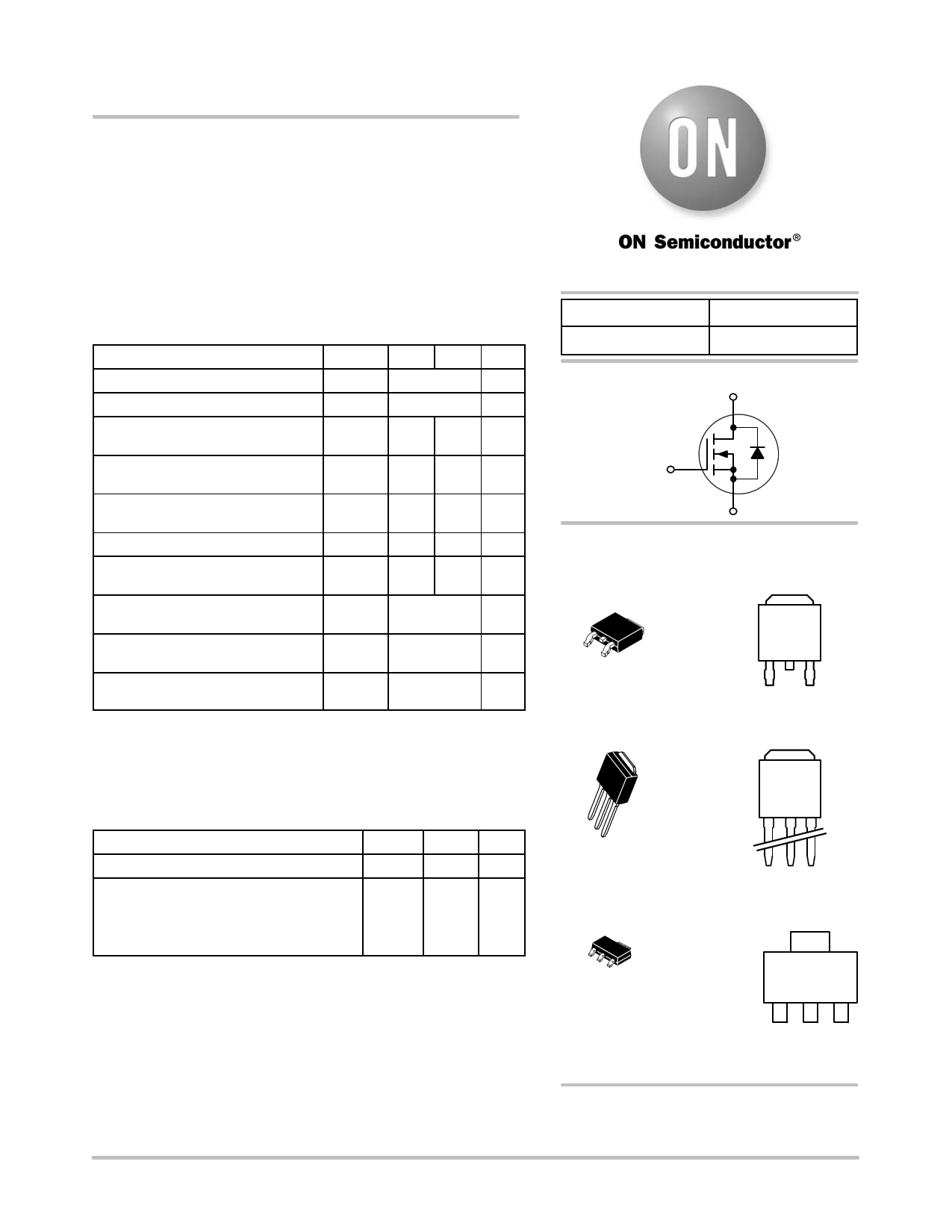
N−Channel MOSFET
D (2)
G (1)
S (3)
MARKING
DIAGRAMS
4
Drain
12
3
4 DPAK
CASE 369C
(Surface Mount)
STYLE 2
1
Gate
2
Drain
3
Source
4
Drain
4
IPAK
CASE 369D
(Straight Lead)
1
2
3
Y
WW
2N40
STYLE 2
= Year
= Work Week
= Device Code
12 3
Gate Drain Source
G = Pb−Free Package
1 23
A
Y
W
2N40
Drain
4 SOT−223
4
CASE 318E
STYLE 3
AYW
2N40G
= Assembly Location
G
= Year
12 3
= Work Week
= Specific Device Code
Gate Drain Source
G = Pb−Free Package
(*Note: Microdot may be in either location)
ORDERING INFORMATION
See detailed ordering and shipping information in the package
dimensions section on page 3 of this data sheet.
Publication Order Number:
NDD02N40/D
1 page 
NDD02N40, NDT02N40
TYPICAL CHARACTERISTICS
1
TJ = 150°C
0.1
TJ = 125°C
1000
100
10
CISS
COSS
CRSS
VGS = 0 V
TJ = 25°C
f = 1 MHz
0.01
0
50 100 150 200 250 300 350 400
VDS, DRAIN−TO−SOURCE VOLTAGE (V)
Figure 7. Drain−to−Source Leakage Current
vs. Voltage
12
11
10
9
8
7
6
5
4 QGS
3
2
1
0
0
QT
QGD
VDS
12
3
450
400
VGS
350
300
250
VDS = 200 V
TJ = 25°C
ID = 1.7 A
200
150
100
50
0
456
QG, TOTAL GATE CHARGE (nC)
Figure 9. Gate−to−Source and
Drain−to−Source Voltage vs. Total Charge
100
10
TJ = 150°C
1
TJ = −55°C
TJ = 25°C
0.1 TJ = 125°C
0.5 0.6 0.7 0.8 0.9 1.0 1.1 1.2 1.3 1.4 1.5 1.6
VSD, SOURCE−TO−DRAIN VOLTAGE (V)
Figure 11. Diode Forward Voltage vs. Current
1
1 10 100
VDS, DRAIN−TO−SOURCE VOLTAGE (V)
Figure 8. Capacitance Variation
100
VGS = 10 V
VDD = 200 V
ID = 1.7 A
td(off)
10 tr
td(on)
tf
1
1 10 100
RG, GATE RESISTANCE (W)
Figure 10. Resistive Switching Time Variation
vs. Gate Resistance
10
VGS ≤ 30 V
Single Pulse
TC = 25°C
10 ms
100 ms
1 ms
1
10 ms
dc
0.1
0.01
0.1
1
RDS(on) Limit
Thermal Limit
Package Limit
10 100
1000
VDS, DRAIN−TO−SOURCE VOLTAGE (V)
Figure 12. Maximum Rated Forward Biased
Safe Operating Area for NDD02N40
http://onsemi.com
5
5 Page | ||
| Páginas | Total 9 Páginas | |
| PDF Descargar | [ Datasheet NDD02N40.PDF ] | |
Hoja de datos destacado
| Número de pieza | Descripción | Fabricantes |
| NDD02N40 | N-Channel Power MOSFET / Transistor | ON Semiconductor |
| Número de pieza | Descripción | Fabricantes |
| SLA6805M | High Voltage 3 phase Motor Driver IC. |
Sanken |
| SDC1742 | 12- and 14-Bit Hybrid Synchro / Resolver-to-Digital Converters. |
Analog Devices |
|
DataSheet.es es una pagina web que funciona como un repositorio de manuales o hoja de datos de muchos de los productos más populares, |
| DataSheet.es | 2020 | Privacy Policy | Contacto | Buscar |