|
|
|
PDF 54ACT715-R Data sheet ( Hoja de datos )
| Número de pieza | 54ACT715-R | |
| Descripción | Programmable Video Sync Generator | |
| Fabricantes | National Semiconductor | |
| Logotipo | ||
Hay una vista previa y un enlace de descarga de 54ACT715-R (archivo pdf) en la parte inferior de esta página. Total 17 Páginas | ||
|
No Preview Available !
December 1998
LM1882•54ACT715
LM1882-R•54ACT715-R Programmable Video Sync
Generator
General Description
The ’ACT715/LM1882 and ’ACT715-R/LM1882-R are 20-pin
TTL-input compatible devices capable of generating Hori-
zontal, Vertical and Composite Sync and Blank signals for
televisions and monitors. All pulse widths are completely de-
finable by the user. The devices are capable of generating
signals for both interlaced and noninterlaced modes of op-
eration. Equalization and serration pulses can be introduced
into the Composite Sync signal when needed.
Four additional signals can also be made available when
Composite Sync or Blank are used. These signals can be
used to generate horizontal or vertical gating pulses, cursor
position or vertical Interrupt signal.
These devices make no assumptions concerning the system
architecture. Line rate and field/frame rate are all a function
of the values programmed into the data registers, the status
register, and the input clock frequency.
The ’ACT715/LM1882 is mask programmed to default to a
Clock Disable state. Bit 10 of the Status Register, Register 0,
defaults to a logic “0”. This facilitates (re)programming be-
fore operation.
The ’ACT715-R/LM1882-R is the same as the ’ACT715/
LM1882 in all respects except that the ’ACT715-R/
LM1882-R is mask programmed to default to a Clock En-
abled state. Bit 10 of the Status Register defaults to a logic
“1”. Although completely (re)programmable, the ’ACT715-R/
LM1882-R version is better suited for applications using the
default 14.31818 MHz RS-170 register values. This feature
allows power-up directly into operation, following a single
CLEAR pulse.
Features
n Maximum Input Clock Frequency > 130 MHz
n Interlaced and non-interlaced formats available
n Separate or composite horizontal and vertical Sync and
Blank signals available
n Complete control of pulse width via register
programming
n All inputs are TTL compatible
n 8 mA drive on all outputs
n Default RS170/NTSC values mask programmed into
registers
n 4 KV minimum ESD immunity
n ’ACT715-R/LM1882-R is mask programmed to default to
a Clock Enable state for easier start-up into
14.31818 MHz RS170 timing
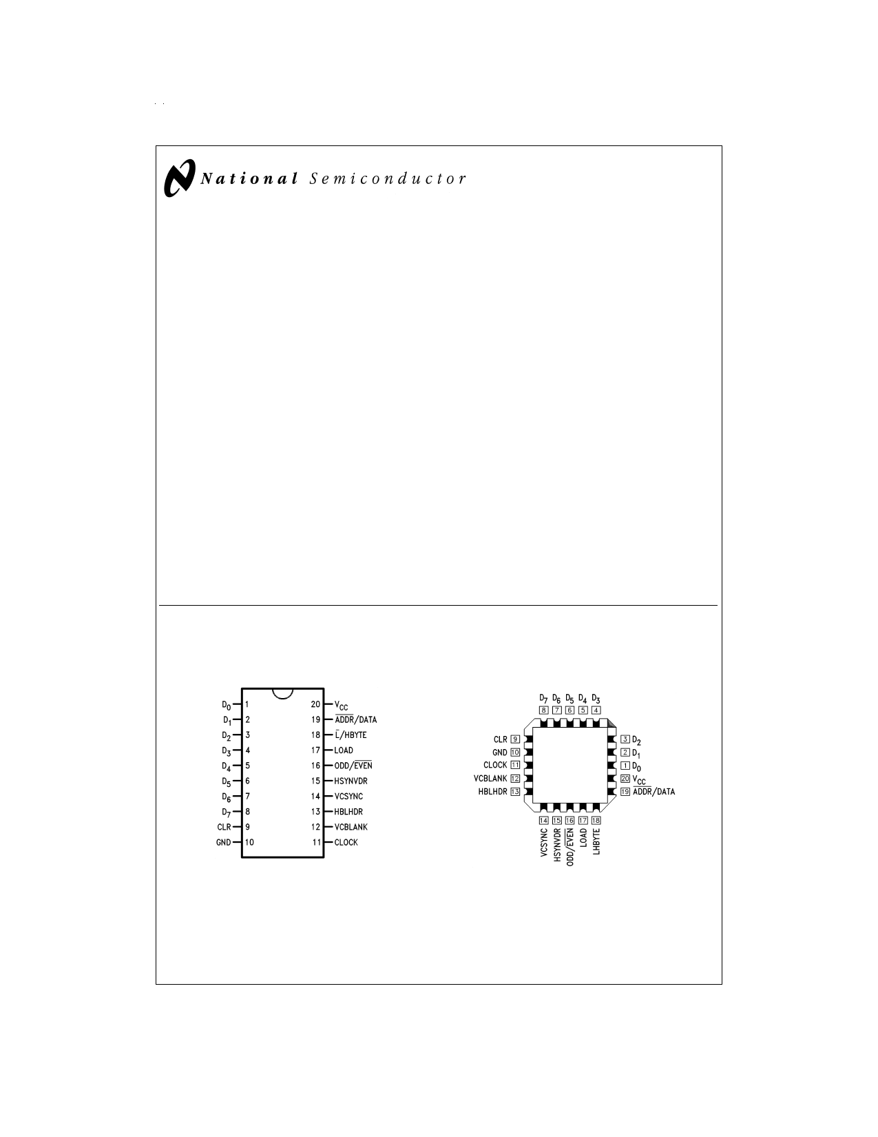
Connection Diagrams
Pin Assignment for
DIP and SOIC
Pin Assignment
for LCC
DS100232-1
Order Number LM1882CN or LM1882CM
For Default RS-170, Order Number
LM1882-RCN or LM1882-RCM
TRI-STATE® is a registered trademark of National Semiconductor Corporation.
FACT™ is a trademark of Fairchild Semiconductor Corporation.
© 1998 National Semiconductor Corporation DS100232
DS100232-2
www.national.com
1 page 
Signal Specification (Continued)
DS100232-5
FIGURE 2. Vertical Waveform Specification
FIGURE 3. Equalization/Serration Interval Programming
DS100232-12
HORIZONTAL AND VERTICAL GATING SIGNALS
Horizontal Drive and Vertical Drive outputs can be utilized as
general purpose Gating Signals. Horizontal and Vertical Gat-
ing Signals are available for use when Composite Sync and
Blank signals are selected and the value of Bit 2 of the Sta-
tus Register is 0. The Vertical Gating signal will change in the
same manner as that specified for the Vertical Blank.
Horizontal Gating Signal Width = [REG(16) − REG(15)] x
ckper
Vertical Gating Signal Width: = [REG(18) − REG(17)] x
hper
CURSOR POSITION AND VERTICAL INTERRUPT
The Cursor Position and Vertical Interrupt signal are avail-
able when Composite Sync and Blank signals are selected
and Bit 2 of the Status Register is set to the value of 1. The
Cursor Position generates a single pulse of n clocks wide
during every line that the cursor is specified. The signals are
generated by logically ORing (ANDing) the active LOW
(HIGH) signals specified by the registers used for generating
Horizontal and Vertical Gating signals. The Vertical Interrupt
signal generates a pulse during the vertical interval speci-
fied. The Vertical Interrupt signal will change in the same
manner as that specified for the Vertical Blanking signal.
Horizontal Cursor Width = [REG(16) − REG(15)] x ckper
Vertical Cursor Width = [REG(18) − REG(17)] x hper
Vertical Interrupt Width = [REG(14) − REG(13)] x hper
Addressing Logic
The register addressing logic is composed of two blocks of
logic. The first is the address register and counter (AD-
DRCNTR), and the second is the address decode (AD-
DRDEC).
ADDRCNTR LOGIC
Addresses for the data registers can be generated by one of
two methods. Manual addressing requires that each byte of
each register that needs to be loaded needs to be ad-
dressed. To load both bytes of all 19 registers would require
a total of 57 load cycles (19 address and 38 data cycles).
Auto Addressing requires that only the initial register value
be specified. The Auto Load sequence would require only 39
load cycles to completely program all registers (1 address
and 38 data cycles). In the auto load sequence the low order
byte of the data register will be written first followed by the
high order byte on the next load cycle. At the time the High
Byte is written the address counter is incremented by 1. The
counter has been implemented to loop on the initial value
loaded into the address register. For example: If a value of 0
was written into the address register then the counter would
count from 0 to 18 before resetting back to 0. If a value of 15
was written into the address register then the counter would
count from 15 to 18 before looping back to 15. If a value
greater than or equal to 18 is placed into the address register
the counter will continuously loop on this value. Auto ad-
dressing is initiated on the falling edge of LOAD when AD-
DRDATA is 0 and LHBYTE is 1. Incrementing and loading of
data registers will not commence until the falling edge of
LOAD after ADDRDATA goes to 1. The next rising edge of
5 www.national.com
5 Page 
Capacitance (Continued)
FIGURE 5. AC Specifications
DS100232-6
Additional Applications Information
POWERING UP
The ’ACT715/LM1882 default value for Bit 10 of the Status
Register is 0. This means that when the CLEAR pulse is ap-
plied and the registers are initialized by loading the default
values the CLOCK is disabled. Before operation can begin,
Bit 10 must be changed to a 1 to enable CLOCK. If the de-
fault values are needed (no other programming is required)
then Figure 6 illustrates a hardwired solution to facilitate the
enabling of the CLOCK after power-up. Should control sig-
nals be difficult to obtain, Figure 7 illustrates a possible solu-
tion to automatically enable the CLOCK upon power-up. Use
of the ’ACT715-R/LM1882-R eliminates the need for most of
this circuitry. Modifications of the Figure 7 circuit can be
made to obtain the lone CLEAR pulse still needed upon
power-up.
Note that, although during a Vectored Restart none of the
preprogrammed registers are affected, some signals are af-
fected for the duration of one frame only. These signals are
the Horizontal and Vertical Drive signals. After a Vectored
Restart the beginning of these signals will occur at the first
CLK. The end of the signals will occur as programmed. At
the completion of the first frame, the signals will resume to
their programmed start and end time.
PREPROGRAMMING “ON-THE-FLY”
Although the ’ACT715/LM1882 and ’ACT715-R/LM1882-R
are completely programmable, certain limitations must be
set as to when and how the parts can be reprogrammed.
Care must be taken when reprogramming any End Time reg-
isters to a new value that is lower than the current value.
Should the reprogramming occur when the counters are at a
count after the new value but before the old value, then the
counters will continue to count up to 4096 before rolling over.
For this reason one of the following two precautions are rec-
ommended when reprogramming “on-the-fly”. The first rec-
ommendation is to reprogram horizontal values during the
horizontal blank interval only and/or vertical values during
the vertical blank interval only. Since this would require deli-
cate timing requirements the second recommendation may
be more appropriate.
The second recommendation is to program a Vectored Re-
start as the final step of reprogramming. This will ensure that
all registers are set to the newly programmed values and
that all counters restart at the first CLK position. This will
avoid overrunning the counter end times and will maintain
the video integrity.
11 www.national.com
11 Page | ||
| Páginas | Total 17 Páginas | |
| PDF Descargar | [ Datasheet 54ACT715-R.PDF ] | |
Hoja de datos destacado
| Número de pieza | Descripción | Fabricantes |
| 54ACT715-R | Programmable Video Sync Generator | National Semiconductor |
| Número de pieza | Descripción | Fabricantes |
| SLA6805M | High Voltage 3 phase Motor Driver IC. |
Sanken |
| SDC1742 | 12- and 14-Bit Hybrid Synchro / Resolver-to-Digital Converters. |
Analog Devices |
|
DataSheet.es es una pagina web que funciona como un repositorio de manuales o hoja de datos de muchos de los productos más populares, |
| DataSheet.es | 2020 | Privacy Policy | Contacto | Buscar |