|
|
|
PDF GA8522 Data sheet ( Hoja de datos )
| Número de pieza | GA8522 | |
| Descripción | 2A Step-Down DC-DC Converter | |
| Fabricantes | Linear Artwork | |
| Logotipo | ||
Hay una vista previa y un enlace de descarga de GA8522 (archivo pdf) en la parte inferior de esta página. Total 20 Páginas | ||
|
No Preview Available !
Linear Artwork
GA8522
300KHz, 2A Step-Down DC-DC Converter
v General Description
The GA8522 is a voltage mode, step-down
DC-DC converter that is designed to meet 2A
output current and utilizes PWM control scheme
that switches with 300KHz fixed frequency. This
device includes a reference voltage source, error
amplifier, oscillation circuit, P-channel MOSFET,
and etc.
The input voltage range of GA8522 is from
3.6V to 23V, and provides adjustable output
voltage range from 0.8V to VIN for customers in
application.
The GA8522 provides an enable function that
can be controlled by external logic signal and
excellent regulation during line or load transient
due to the internal compensation. Other features
of thermal protection, current limit and short
circuit protection are also included. Due to the
low Drain-Source resistance of internal power
MOSFET, the GA8522 provides a high efficiency
step-down application. It can also operate with a
maximum duty cycle of 100% for use in low
drop-out conditions.
The package is available in a standard
SOP-8L.
v Features
• Adjustable Output Voltage from 0.8V to VIN
• Operating Input Voltage up to 23V
• Great Output Capability: 2A
• Oscillation Frequency: 300KHz
• Built-in P-channel MOSFET
• External ON/OFF Control Function
• Low Shutdown Current: 1uA
• Current Limit and Thermal Protection
• Short Circuit Protection
• Stable With Low ESR Output Ceramic Capacitor
• SOP-8L Package
• All Products meet Rohs Standard
v Applications
• Broadband Communication Device
• LCD TV / Monitor
• Storage Device
• Wireless Application
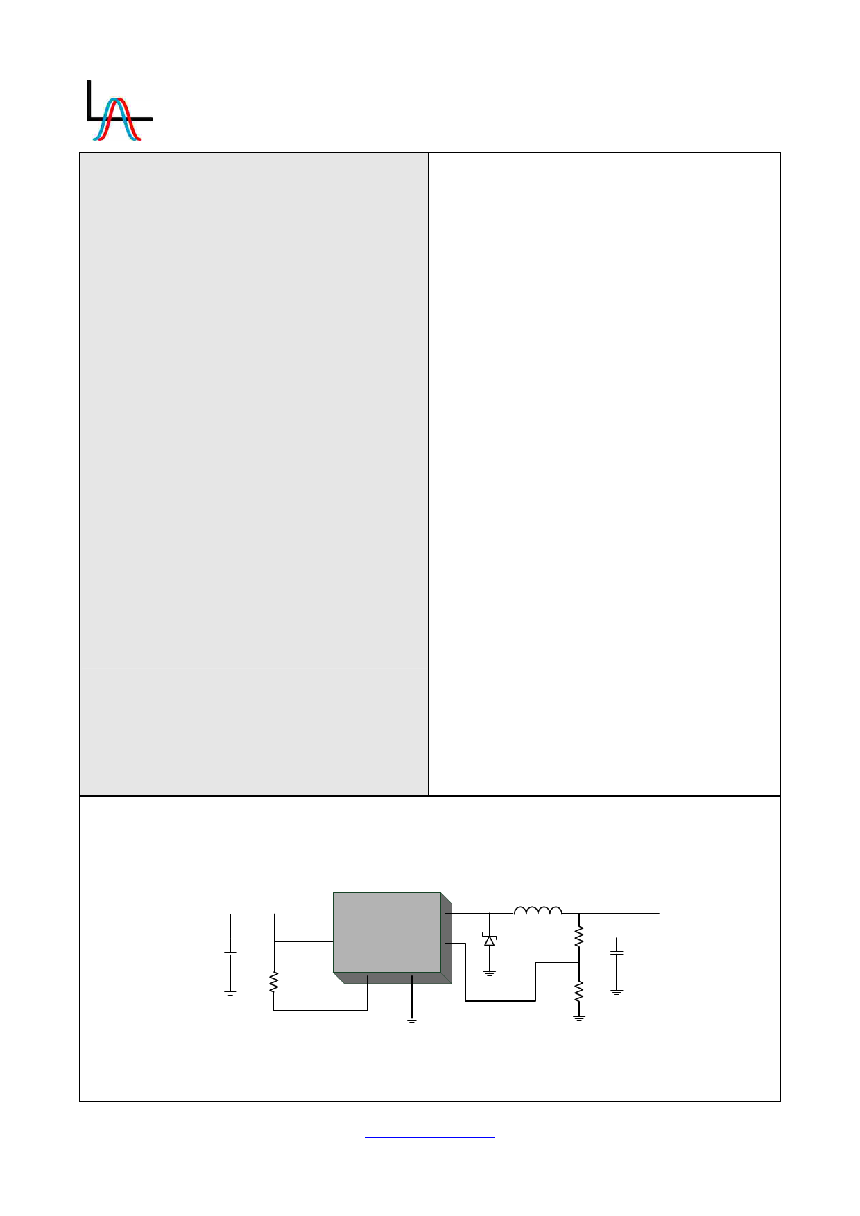
v Typical Application
VIN
CIN
GA8522
IN SW
4
EN
2
FB
OCSET GND
ROCSET
3 7,8
5,6
1
L1
D1
VOUT
R1
COUT
R2
GA8522-B01
* VOUT = VFB x ( 1 + R1 / R2 )
© Linear Artwork, Inc.
www.linear-artwork.com
-1-
Apr. 01, 2008
1 page 
Linear Artwork
GA8522
300KHz, 2A Step-Down DC-DC Converter
v Electrical Specifications
VIN=12V, VOUT set to 3.3V, TA=25ºC, unless otherwise noted.
Parameter
Symbol Test Condition
Feedback Voltage
VFB
ILOAD=0.1A
Efficiency
VIN=12V, VOUT=5V, ILOAD=2A
η
VIN=5V, VOUT=3.3V, ILOAD=2A
Oscillation Frequency FOSC
Frequency of Short
Circuit Protection
FSCP
Duty Cycle
DC
VIN=3.6~23V, ILOAD=0.2A~2A
VIN=3.6~23V
VFB=0V force driver on
VFB=1.5V force driver off
Internal MOSFET On
Resistance
RDS(ON)
VIN=5V, VFB=0V
VIN=12V, VFB=0V
Quiescent Current
IQ
VIN=3.6V~23V, VFB=1.5V force drive off
Shutdown Current
IS
EN pin = GND
EN Pin Input
Threshold Voltage
VEN
Regulator OFF
Regulator ON
EN Pin Bias Current IEN
Regulator OFF
Regulator ON
FB Pin Bias Current
OCSET Pin Bias
Current
Line Regulation
IFB
IOCSET
△VLINE
ILOAD=0.2A
ILOAD=0.2A
VIN=3.6V~23V, ILOAD =0.2A
Load Regulation
△VLOAD
Over Temperature
Shutdown
Over Temperature
Shutdown Hysteresis
TSD
THYS
ILOAD=0.2A~2A
Min Typ Max Units
0.784 0.8 0.816 V
92
%
89
240 300 360 KHz
30 50 70 KHz
100
%
0
160 180
mΩ
100 120
3 10 mA
1 10 uA
0.8
1.3 V
2.0
1
uA
20
0.1 0.5 uA
75 90 105 uA
2%
0.1 %
150 oC
25 oC
GA8522-B01
© Linear Artwork, Inc.
www.linear-artwork.com
-5-
Apr. 01, 2008
5 Page 
Linear Artwork
GA8522
300KHz, 2A Step-Down DC-DC Converter
SW
FB
GND
C SNU B
RSNUB
VOUT
The power dissipation across this device can be
calculated by the following formula:
PD = (ILOAD)2 x RDS(ON) x D + 1/2 x VIN x IOUT x
(tr+tf) x fS + QGate x VGS x fS + IQ x VIN
Choose the value of RC network by the following
procedure:
(1) Measure the voltage ringing frequency (fR)
of the SW pin.
(2) Find a small capacitor and place it across
the SW pin and the GND pin to damp the
ringing frequency by half.
(3) The parasitical capacitance (CPAR) at the
SW pin is 1/3 the value of the added
capacitance above. The parasitical
inductance (LPAR) at the SW pin is:
1
LPAR = ( 2πfR )2 × CPAR
(4) Select the value of CSNUB that should be
more than 2~4 times the value of CPAR but
must be small enough so that the power
dissipation of RSNUB is kept to a minimum.
The power rating of RSNUB can be
calculated by following formula:
P _ RSNUB = CSNUB ×VIN 2 × fS
Where:
D: Duty Cycle
fS: Switching Frequency
VGS: Power MOSFET Gate Voltage
IQ: Quiescent Current
The tr, tf, and QGate are the rising, falling time,
and gate charge of the internal power switch.
The typical value of (tr+tf) is approximately 28ns,
and the QGate is approximately 10nC. The VGS is
approximately equal VIN.
The maximum power dissipation of this device
depends on the thermal resistance of the IC
package and PCB layout, the temperature
difference between the die junction and ambient
air, and the rate of airflow. The maximum power
dissipation can be calculated by the following
formula:
PD(MAX) = (TJ -TA ) / θJA
Where TJ -TA is the temperature difference
between the die junction and surrounding
environment, θJA is the thermal resistance from
the junction to the surrounding environment.
(5) Calculate the value of RSNUB by the
following formula and adjust the value to
meet the expectative peak voltage.
RSNUB = 2π × fR × LPAR
Thermal Considerations
Thermal protection limits total power dissipation
in this device. When the junction temperature
reaches approximately 150oC, the thermal
sensor signals the shutdown logic turning off this
device. The thermal sensor will turn this device
on again after the IC's junction temperature
cools by 25oC.
For continuous operation, do not exceed the
maximum operation junction temperature 125oC.
The value of junction to case thermal resistance
θJC is also popular to users. This thermal
parameter is convenient for users to estimate the
internal junction operated temperature of
packages while IC operating. The operated
junction temperature can be calculated by the
following formula:
TJ = TC + PD x θJC
TC is the package case temperature measured
by thermal sensor. Therefore it's easy to
estimate the junction temperature by any
condition.
There are many factors affect the thermal
resistance. Some of these factors include trace
width, copper thickness, total PCB copper area,
and etc.
GA8522-B01
© Linear Artwork, Inc.
www.linear-artwork.com
- 11 -
Apr. 01, 2008
11 Page | ||
| Páginas | Total 20 Páginas | |
| PDF Descargar | [ Datasheet GA8522.PDF ] | |
Hoja de datos destacado
| Número de pieza | Descripción | Fabricantes |
| GA8522 | 2A Step-Down DC-DC Converter | Linear Artwork |
| Número de pieza | Descripción | Fabricantes |
| SLA6805M | High Voltage 3 phase Motor Driver IC. |
Sanken |
| SDC1742 | 12- and 14-Bit Hybrid Synchro / Resolver-to-Digital Converters. |
Analog Devices |
|
DataSheet.es es una pagina web que funciona como un repositorio de manuales o hoja de datos de muchos de los productos más populares, |
| DataSheet.es | 2020 | Privacy Policy | Contacto | Buscar |