|
|
|
PDF NCV47551 Data sheet ( Hoja de datos )
| Número de pieza | NCV47551 | |
| Descripción | 3.3V to 20V Adjustable Low Noise LDO Regulator | |
| Fabricantes | ON Semiconductor | |
| Logotipo | ||
Hay una vista previa y un enlace de descarga de NCV47551 (archivo pdf) en la parte inferior de esta página. Total 12 Páginas | ||
|
No Preview Available !
NCV47551
3.3 V to 20 V Adjustable
Low Noise LDO Regulator
with Adjustable Current
Limit and 3.3 V Logic
Compatible Enable Input
The NCV47551 is a low noise low output current integrated low
dropout regulator designed for use in harsh automotive environments.
It includes wide operating temperature and input voltage ranges. The
device is offered with adjustable voltage versions available in 3%
output voltage accuracy. It has a high peak input voltage tolerance and
reverse input voltage protection. It also provides overcurrent
protection, overtemperature protection and enable for control of the
state of the output voltage. The integrated current sense feature
provides diagnosis and system protection functionality. The current
limit of the device is adjustable by resistor connected to CSO pin.
Voltage on CSO pin is proportional to output current.
Features
• Adjustable Voltage Version (from 3.3 V to 20 V) ± 3% Output
Voltage
• Enable Input (3.3 V Logic Compatible Thresholds)
• Adjustable Current Limit (from 100 mA to 20 mA) with 10%
Accuracy
• Protection Features:
♦ Current Limitation
♦ Thermal Shutdown
♦ Reverse Input Voltage
• This is a Pb−Free Device
Typical Applications
• Microphone Power Supply
• Audio and Infotainment System
• Navigation
• Satellite Radio
http://onsemi.com
8
1
SOIC−8
SUFFIX D
CASE 751
MARKING
DIAGRAM
8
47551
ALYW
G
1
47551
A
L
Y
W
G
= Specific Device Code
= Assembly Location
= Wafer Lot
= Year
= Work Week
= Pb−Free Package
ORDERING INFORMATION
See detailed ordering and shipping information in the package
dimensions section on page 11 of this data sheet.
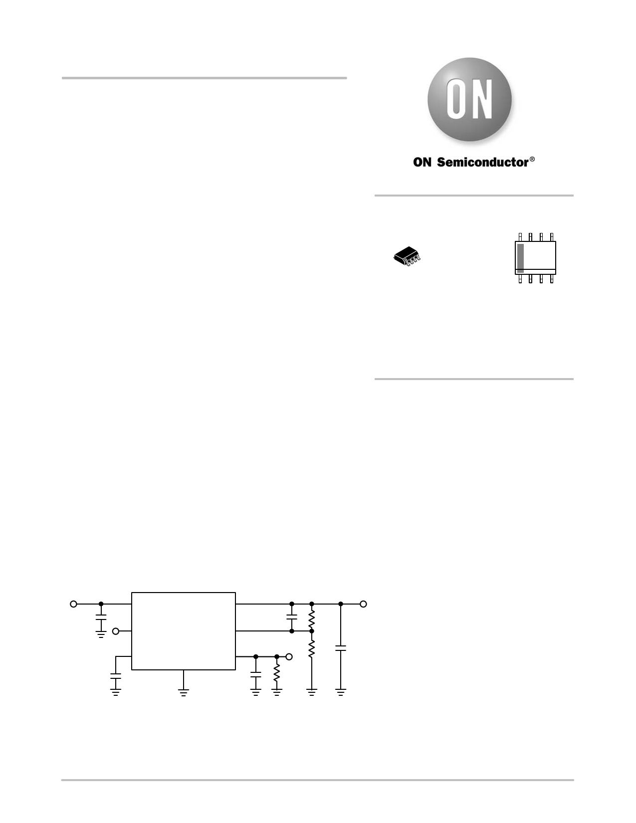
Cin
1 mF
Vin Vout
EN
NCV47551
ADJ
Cb*
R1
Cnoise*
NR
GND
CSO
CCSO
1 mF
RCSO
R2
Cb*, Cnoise* − Optional for noise reduction.
Figure 1. Application Schematic
(See Application Section for more details)
Cout
10 mF
© Semiconductor Components Industries, LLC, v2013
December, 2013 − Rev. 0
1
Publication Order Number:
NCV47551/D
1 page 
NCV47551
ELECTRICAL CHARACTERISTICS Vin = 13.5 V, VEN = 3.3 V, RCSO = 0 W, CCSO = 1 mF, Cin = 1 mF, Cout = 10 mF, ESR = 1.5 W, Min
and Max values are valid for temperature range −40°C ≤ TJ ≤ +150°C unless noted otherwise and are guaranteed by test, design or
statistical correlation. Typical values are referenced to TJ = 25°C. Output Current Iout is the current out of pin including current through the
resistor divider R1 and R2. (Note 7)
Parameter
Test Conditions
Symbol Min Typ Max Unit
OUTPUT CURRENT SENSE
CSO Voltage Level at Current
Limit
Vout = 0.9 x Vout_nom, (Vout_nom = 5 V)
RCSO = 220 W
VCSO_Ilim
2.346
(−8 %)
2.55
2.754
(+8 %)
V
CSO Transient Voltage Level
CCSO = 4.7 mF, RCSO = 220 W
Iout pulse from 0.1 mA to 20 mA, tr = 1 ms
VCSO − − 3.3 V
Output Current to CSO Current
Ratio (Note 11)
VCSO = 2 V
Iout = 0.1 mA to 20 mA, (Vout_nom = 5 V)
Iout/ICSO
−
(−10%)
(1/1)
−
(+10%)
−
CSO Current at no Load Current
(Note 12)
THERMAL SHUTDOWN
VCSO = 0 V
R1 = 82 kW, R2 = 27 kW, Cb = 10 nF
ICSO_off
−
47 60 mA
Thermal Shutdown Temperature
(Note 10)
Iout = 1 mA
TSD 150 − 195 °C
Product parametric performance is indicated in the Electrical Characteristics for the listed test conditions, unless otherwise noted. Product
performance may not be indicated by the Electrical Characteristics if operated under different conditions.
7. Performance guaranteed over the indicated operating temperature range by design and/or characterization tested at TA ≈ TJ. Low duty
cycle pulse techniques are used during testing to maintain the junction temperature as close to ambient as possible.
8. Vin_min = 4.4 V or (Vout_nom + 1 V), whichever is higher.
9. Measured when the output voltage Vout has dropped – 2% from the nominal value obtained at Vin = Vout_nom + 8.5 V.
10. Values based on design and/or characterization.
11. Not guaranteed in dropout.
12. ICSO current at no load includes also mirrored current of resistor divider (Idiv = Vout / (R1 + R2)).
http://onsemi.com
5
5 Page 
NCV47551
Thermal Considerations
As power in the NCV47551 increases, it might become
necessary to provide some thermal relief. The maximum
power dissipation supported by the device is dependent
upon board design and layout. Mounting pad configuration
on the PCB, the board material, and the ambient temperature
affect the rate of junction temperature rise for the part. When
the NCV47551 has good thermal conductivity through the
PCB, the junction temperature will be relatively low with
high power applications. The maximum dissipation the
NCV47551 can handle is given by:
ƪ ƫTJ(MAX) * TA
PD(MAX) +
RqJA
(eq. 5)
240
220
200
180
160 1 oz, Single Layer
140
120 2 oz, Single Layer
100
0
100 200 300 400 500 600 700
COPPER HEAT SPREADER AREA (mm2)
Figure 19. Thermal Resistance vs. PCB Copper Area
Since TJ is not recommended to exceed 150°C, then the
NCV47551 in SO-8 soldered on 645 mm2, 1 oz copper area,
FR4 can dissipate up to 0.94 W when the ambient
temperature (TA) is 25°C. See Figure 19 for RthJA versus
PCB area. The power dissipated by the NCV47551 can be
calculated from the following equations:
PD [ VinǒIq@IoutǓ ) IoutǒVin * VoutǓ
(eq. 6)
or
Vin(MAX)
[
PD(MAX) )
Iout
ǒVout
) Iq
IoutǓ
(eq. 7)
Hints
Vin and GND printed circuit board traces should be as
wide as possible. When the impedance of these traces is
high, there is a chance to pick up noise or cause the regulator
to malfunction. Place external components, especially the
output capacitor, as close as possible to the NCV47551 and
make traces as short as possible.
ORDERING INFORMATION
Device
Output Voltage
Marking
Package
Shipping†
NCV47551DAJR2G
Adjustable
47551
SOIC−8
(Pb−Free)
2500 / Tape & Reel
†For information on tape and reel specifications, including part orientation and tape sizes, please refer to our Tape and Reel Packaging
Specifications Brochure, BRD8011/D.
http://onsemi.com
11
11 Page | ||
| Páginas | Total 12 Páginas | |
| PDF Descargar | [ Datasheet NCV47551.PDF ] | |
Hoja de datos destacado
| Número de pieza | Descripción | Fabricantes |
| NCV47551 | 3.3V to 20V Adjustable Low Noise LDO Regulator | ON Semiconductor |
| Número de pieza | Descripción | Fabricantes |
| SLA6805M | High Voltage 3 phase Motor Driver IC. |
Sanken |
| SDC1742 | 12- and 14-Bit Hybrid Synchro / Resolver-to-Digital Converters. |
Analog Devices |
|
DataSheet.es es una pagina web que funciona como un repositorio de manuales o hoja de datos de muchos de los productos más populares, |
| DataSheet.es | 2020 | Privacy Policy | Contacto | Buscar |