|
|
|
PDF NCV8715 Data sheet ( Hoja de datos )
| Número de pieza | NCV8715 | |
| Descripción | Low Dropout Linear Voltage Regulator | |
| Fabricantes | ON Semiconductor | |
| Logotipo | ||
Hay una vista previa y un enlace de descarga de NCV8715 (archivo pdf) en la parte inferior de esta página. Total 20 Páginas | ||
|
No Preview Available !
NCV8715
50 mA Ultra-Low Iq, Wide
Input Voltage, Low Dropout
Linear Voltage Regulator
The NCV8715 is 50 mA LDO Linear Voltage Regulator. It is a very
stable and accurate device with ultra−low ground current consumption
(4.7 mA over the full output load range) and a wide input voltage range
(up to 24 V). The regulator incorporates several protection features
such as Thermal Shutdown and Current Limiting.
Features
• Operating Input Voltage Range: 2.5 V to 24 V
• Fixed Voltage Options Available: 1.2 V to 5.0 V
• Ultra Low Quiescent Current: Max. 5.8 mA Over Full Load and
Temperature
• ±2% Accuracy Over Full Load, Line and Temperature Variations
• PSRR: 52 dB at 100 kHz
• Noise: 190 mVRMS from 200 Hz to 100 kHz
• Thermal Shutdown and Current Limit protection
• Available in XDFN6 1.5 x 1.5 mm and SC−70 (SC−88A) Package
• These are Pb−Free Devices
Typical Applications
• Infotainment, Audio
• Communication Systems
• Safety Systems
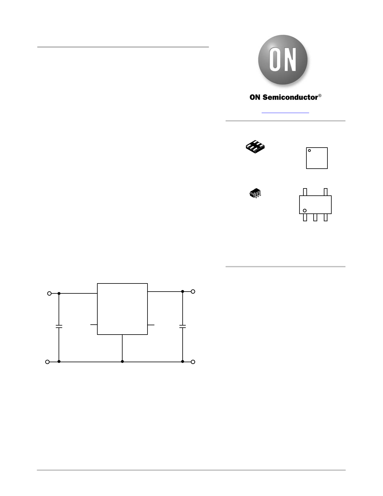
2.5 V < Vout < 24 V
IN
OUT
1.2 V < Vout < 5 V
1 mF
Ceramic
NCV8715
NC NC
GND
1 mF
Ceramic
www.onsemi.com
XDFN6
CASE 711AE
MARKING
DIAGRAMS
1
XXXMG
G
SC−70−5
(SC−88A)
CASE 419A
XXX MG
G
XXX
M
G
= Specific Device Code
= Date Code
= Pb−Free Package
(Note: Microdot may be in either location)
ORDERING INFORMATION
See detailed ordering, marking and shipping information on
page 18 of this data sheet.
Figure 1. Typical Application Schematic
© Semiconductor Components Industries, LLC, 2015
August, 2015 − Rev. 4
1
Publication Order Number:
NCV8715/D
1 page 
NCV8715
ELECTRICAL CHARACTERISTICS − Voltage Version 1.5 V
−40°C ≤ TJ ≤ 125°C; VIN = 2.5 V; IOUT = 1 mA, CIN = COUT = 1.0 mF, unless otherwise noted. Typical values are at TJ = +25°C. (Note 11)
Parameter
Test Conditions
Symbol Min Typ Max Unit
Operating Input Voltage
IOUT ≤ 10 mA
VIN 2.5
24 V
Output Voltage Accuracy
Line Regulation
Load Regulation
Dropout Voltage (Note 9)
Maximum Output Current
Ground Current
Power Supply Rejection Ratio
Output Noise Voltage
Thermal Shutdown Temperature
(Note 10)
10 mA < IOUT < 50 mA
3.0 24
3.0 V < VIN < 24 V, 0 < IOUT < 50 mA
VOUT
1.455 1.5 1.545
V
VOUT + 1 V ≤ VIN ≤ 24 V, IOUT = 1 mA
RegLINE
2 10 mV
IOUT = 0 mA to 50 mA
RegLOAD
5 10 mV
VDO
− mV
(Note 12)
IOUT
100
200 mA
0 < IOUT < 50 mA, VIN = 24 V
IGND
3.4 5.8 mA
VIN = 3.0 V, VOUT = 1.5 V f = 100 kHz PSRR 56 dB
VPP = 200 mV modulation
IOUT = 1 mA, COUT = 10 mF
VOUT = 1.5 V, IOUT = 50 mA
f = 200 Hz to 100 kHz, COUT = 10 mF
VN
75 mVrms
Temperature increasing from TJ = +25°C
TSD
170 °C
Thermal Shutdown Hysteresis
(Note 10)
Temperature falling from TSD
TSDH
− 15
− °C
9. Not Characterized at VIN = 3.0 V, VOUT = 1.5 V, IOUT = 50 mA.
10. Guaranteed by design and characterization.
11. Performance guaranteed over the indicated operating temperature range by design and/or characterization production tested at
TJ = TA = 25°C. Low duty cycle pulse techniques are used during testing to maintain the junction temperature as close to ambient as possible.
12. Respect SOA.
www.onsemi.com
5
5 Page 
NCV8715
1.2
1.199
VIN = 3.0 V
1.198
1.197
1.196
1.195
VIN = (5.0 − 24.0) V
1.194
NCV8715x12xxx
1.193
1.192
CIN = COUT = 1 mF
IOUT = 1 mA
−40 −20 0 20
40 60
80 100 120
TEMPERATURE (°C)
Figure 4. Output Voltage vs. Temperature
2.506
2.504
VIN = 3.0 V
2.502
2.5
2.498
VIN = (5.0 − 24.0) V
2.496
2.494 NCV8715x25xxx
2.492
CIN = COUT = 1 mF
IOUT = 1 mA
2.49
−40 −20 0
20
40 60
80 100 120
TEMPERATURE (°C)
Figure 5. Output Voltage vs. Temperature
3.318
3.315
3.312
3.309
3.306
3.303
3.3
3.297
3.294
−40
NCV8715x33xxx
CIN = COUT = 1 mF
IOUT = 1 mA
VIN = 4.3 V to 24 V
−20 0 20 40 60 80 100 120
TEMPERATURE (°C)
Figure 6. Output Voltage vs. Temperature
5.02
5.015
5.01 VIN = (8.0 − 24.0) V
5.005
5
VIN = 6.0 V
4.995
4.99
4.985
NCV8715x50xxx
CIN = COUT = 1 mF
IOUT = 1 mA
4.98
−40 −20 0
20 40 60 80 100 120
JUNCTION TEMPERATURE (°C)
Figure 7. Output Voltage vs. Temperature
1.204
1.200
1.196
NCV8715x12xxx
CIN = COUT = 1 mF
TA = 25°C
2.504
2.500
2.496
NCV8715x25xxx
CIN = COUT = 1 mF
TA = 25°C
1.192
2.492
1.188
1.184
VIN = 3.0 V
VIN = 5.0 V
1.180
VIN = 10 V
VIN = 15 V
1.176
VIN = 20 V
1.172
VIN = 24 V
0 10 20 30 40
OUTPUT CURRENT (mA)
Figure 8. Output Voltage vs. Output Current
50
2.488
2.484
VIN = 3.5 V
VIN = 5.0 V
2.480
VIN = 10 V
VIN = 15 V
2.476
VIN = 20 V
2.472
VIN = 24 V
0 10 20 30 40 50
OUTPUT CURRENT (mA)
Figure 9. Output Voltage vs. Output Current
www.onsemi.com
11
11 Page | ||
| Páginas | Total 20 Páginas | |
| PDF Descargar | [ Datasheet NCV8715.PDF ] | |
Hoja de datos destacado
| Número de pieza | Descripción | Fabricantes |
| NCV8715 | Low Dropout Linear Voltage Regulator | ON Semiconductor |
| NCV8716 | Wide Input Voltage Low Dropout Regulator | ON Semiconductor |
| Número de pieza | Descripción | Fabricantes |
| SLA6805M | High Voltage 3 phase Motor Driver IC. |
Sanken |
| SDC1742 | 12- and 14-Bit Hybrid Synchro / Resolver-to-Digital Converters. |
Analog Devices |
|
DataSheet.es es una pagina web que funciona como un repositorio de manuales o hoja de datos de muchos de los productos más populares, |
| DataSheet.es | 2020 | Privacy Policy | Contacto | Buscar |