|
|
|
PDF IRF7526D1PbF Data sheet ( Hoja de datos )
| Número de pieza | IRF7526D1PbF | |
| Descripción | MOSFET & Schottky Diode | |
| Fabricantes | International Rectifier | |
| Logotipo | ||
Hay una vista previa y un enlace de descarga de IRF7526D1PbF (archivo pdf) en la parte inferior de esta página. Total 10 Páginas | ||
|
No Preview Available !
PD -95437
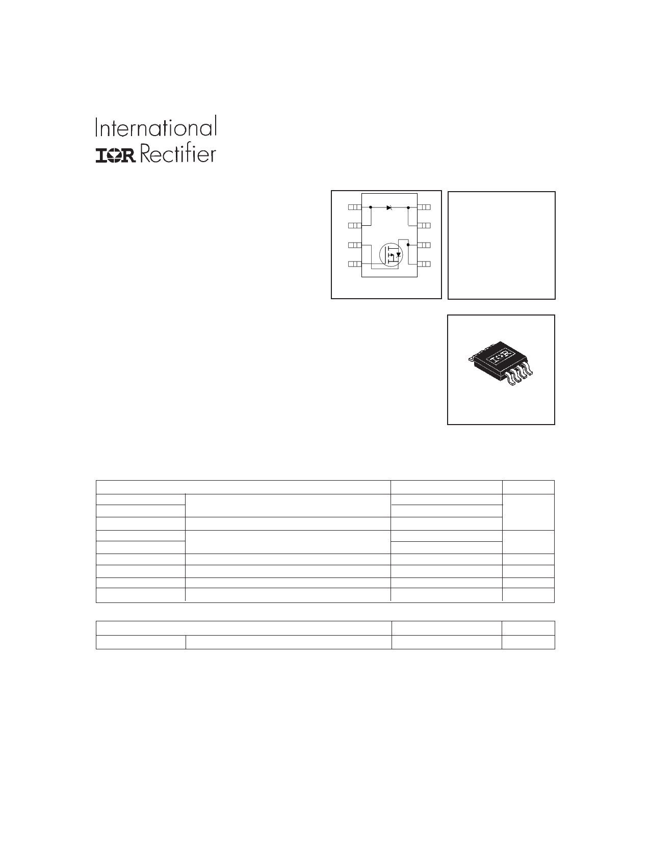
IRF7526D1PbF
l Co-packaged HEXFET® Power
MOSFET and Schottky Diode
l P-Channel HEXFET
l Low VF Schottky Rectifier
l Generation 5 Technology
l Micro8TM Footprint
l Lead-Free
Description
FETKY TM MOSFET & Schottky Diode
A1
A2
8K
7K
VDSS = -30V
S3
6 D RDS(on) = 0.20Ω
G4
5D
Schottky Vf = 0.39V
Top View
The FETKYTM family of co-packaged HEXFETs and Schottky diodes offer the
designer an innovative board space saving solution for switching regulator
applications. Generation 5 HEXFETs utilize advanced processing techniques to
achieve extremely low on-resistance per silicon area. Combining this technology
with International Rectifier's low forward drop Schottky rectifiers results in an
extremely efficient device suitable for use in a wide variety of portable electronics
applications like cell phone, PDA, etc.
The new Micro8TM package, with half the footprint area of the standard SO-8, provides
the smallest footprint available in an SOIC outline. This makes the Micro8TM an ideal
device for applications where printed circuit board space is at a premium. The low
profile (<1.1mm) of the Micro8TM will allow it to fit easily into extremely thin application
environments such as portable electronics and PCMCIA cards.
Micro8TM
Absolute Maximum Ratings
ID @ TA = 25°C
ID @ TA = 70°C
IDM
PD @TA = 25°C
PD @TA = 70°C
VGS
dv/dt
TJ, TSTG
Parameter
Continuous Drain Current, VGS @ -4.5V
Pulsed Drain Current À
Power Dissipation
Linear Derating Factor
Gate-to-Source Voltage
Peak Diode Recovery dv/dt Á
Junction and Storage Temperature Range
Thermal Resistance Ratings
Parameter
RθJA
Junction-to-Ambient Ã
Maximum
-2.0
-1.6
-16
1.25
0.8
10
± 20
-5.0
-55 to +150
Maximum
100
Units
A
W
mW/°C
V
V/ns
°C
Units
°C/W
Notes:
Repetitive rating – pulse width limited by max. junction temperature (see Fig. 9)
ISD ≤ -1.2A, di/dt ≤ 160A/µs, VDD ≤ V(BR)DSS, TJ ≤ 150°C
Pulse width ≤ 300µs – duty cycle ≤ 2%
When mounted on 1 inch square copper board to approximate typical multi-layer PCB thermal resistance
www.irf.com
1
02/22/05
1 page 
IRF7526D1PbF
Power Mosfet Characteristics
1000
100
D = 0.50
0.20
10 0.10
0.05
0.02
0.01
1
0.1
0.00001
PDM
SINGLE PULSE
(THERMAL RESPONSE)
0.0001
0.001
t1
t2
Notes:
1. Duty factor D = t1 / t 2
2. Peak T J = P DM x Z thJC + TC
0.01 0.1
1
t1 , Rectangular Pulse Duration (sec)
10
100
Fig 9. Maximum Effective Transient Thermal Impedance, Junction-to-Ambient
1.5
1.0
VGS = -4.5V
0.5
VGS = -10V
0.0 A
01234
-ID , Drain Current (A)
Fig 10. Typical On-Resistance Vs. Drain
Current
www.irf.com
0.60
0.50
0.40
I = -2.0A
0.30
0.20
0.10
3
A
6 9 12 15
-VGS , Gate-to-Source Voltage (V)
Fig 11. Typical On-Resistance Vs. Gate
Voltage
5
5 Page | ||
| Páginas | Total 10 Páginas | |
| PDF Descargar | [ Datasheet IRF7526D1PbF.PDF ] | |
Hoja de datos destacado
| Número de pieza | Descripción | Fabricantes |
| IRF7526D1PbF | MOSFET & Schottky Diode | International Rectifier |
| Número de pieza | Descripción | Fabricantes |
| SLA6805M | High Voltage 3 phase Motor Driver IC. |
Sanken |
| SDC1742 | 12- and 14-Bit Hybrid Synchro / Resolver-to-Digital Converters. |
Analog Devices |
|
DataSheet.es es una pagina web que funciona como un repositorio de manuales o hoja de datos de muchos de los productos más populares, |
| DataSheet.es | 2020 | Privacy Policy | Contacto | Buscar |