|
|
|
PDF NCP1589D Data sheet ( Hoja de datos )
| Número de pieza | NCP1589D | |
| Descripción | Low Voltage Synchronous Buck Controller | |
| Fabricantes | ON Semiconductor | |
| Logotipo | ||
Hay una vista previa y un enlace de descarga de NCP1589D (archivo pdf) en la parte inferior de esta página. Total 8 Páginas | ||
|
No Preview Available !
NCP1589D
Low Voltage Synchronous
Buck Controller with Light
Load Efficiency and
Transient Enhancement
The NCP1589D is a low cost PWM controller designed to operate
from a 5 V or 12 V supply. This device is capable of producing an
output voltage as low as 0.8 V and converting voltage from as low as
2.5 V. It is easy to operate and provides an optimal level of integration
to reduce size and cost of the power supply. It operates in Ramp Pulse
Modulation mode for superior load step and release response. In
addition to fast transient response, it also includes a 1.5 A gate driver
design and light load efficiency features such as adaptive non−overlap
circuitry and diode emulation. It normally operates at a range of
200−500 kHz in continuous current conduction mode, which reduces
with current at light load for further power saving. Protection features
include programmable overcurrent protection, output overvoltage and
undervoltage protection and input undervoltage lockout (UVLO).
Features
• VCC Range from 4.5 V to 13.2 V
• Adjustable Operating frequency
• Boost Pin Operates to 35 V
• Ramp Pulse Modulation Control
• Precision 0.8 V Internal Reference
• Adjustable Output Voltage
• Internal 1.5 A Gate Drivers
• 80% Max Duty Cycle
• Input Under Voltage Lockout
• Programmable Current Limit
• Adaptive Diode Mode Emulation in Light Load
• This is a Pb−Free Device
Applications
• Graphics Cards
• Desktop Computers
• Servers / Networking
• DSP & FPGA Power Supply
• DC−DC Regulator Modules
www.onsemi.com
MARKING
DIAGRAM
DFN10
CASE 485C
1589D
ALYWG
G
1589D
A
L
Y
W
G
= Specific Device Code
= Assembly Location
= Wafer Lot
= Year
= Work Week
= Pb−Free Device
(Note: Microdot may be in either location)
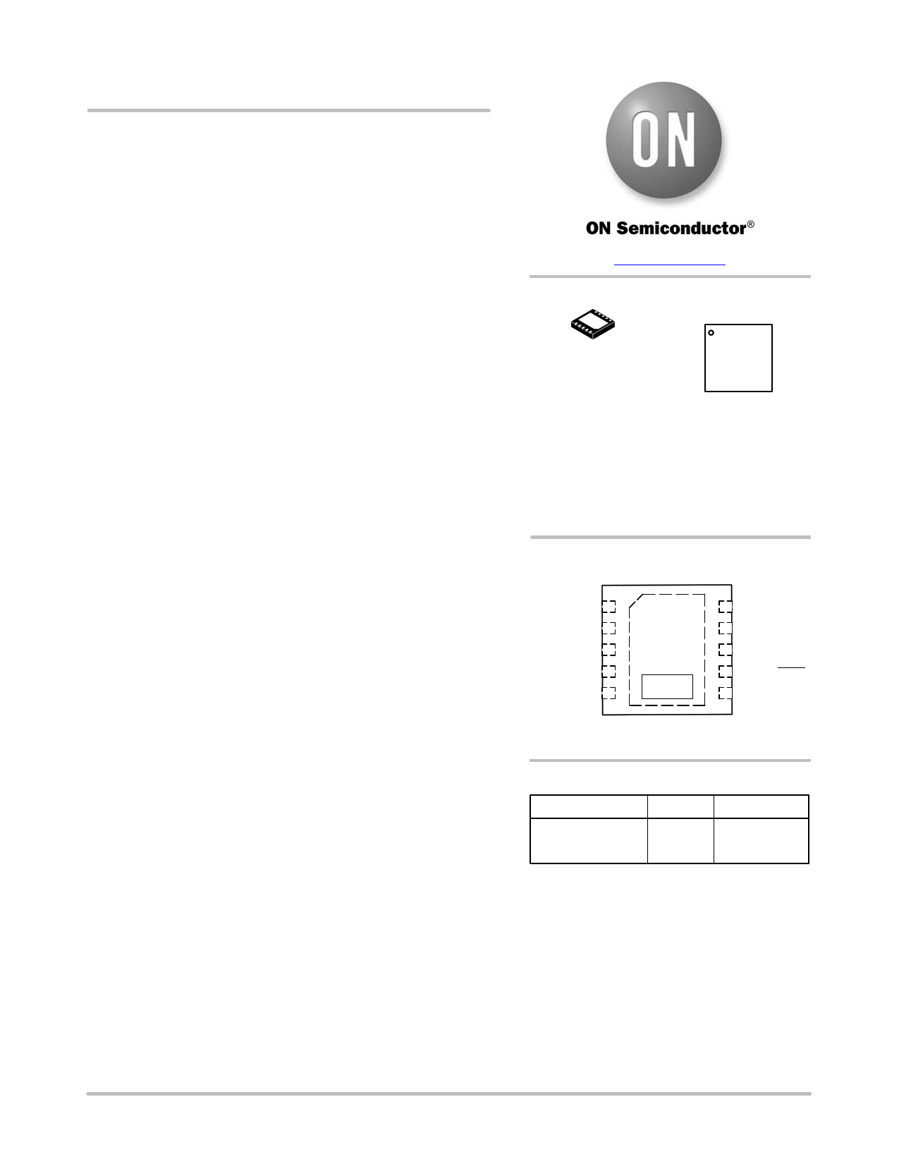
PIN CONNECTIONS
BOOT
LX
UG
LG
GND
1
2
3
4
5
Flag
10 PGOOD
9 VORPM
8 FB
7 COMP/DISB
6 VCC
(Top View)
ORDERING INFORMATION
Device
Package
Shipping†
NCP1589DMNTWG DFN10
3000 /
(Pb−Free) Tape & Reel
†For information on tape and reel specifications,
including part orientation and tape sizes, please
refer to our Tape and Reel Packaging Specifications
Brochure, BRD8011/D.
© Semiconductor Components Industries, LLC, 2017
January, 2017 − Rev. 2
1
Publication Order Number:
NCP1589D/D
1 page 
NCP1589D
ELECTRICAL CHARACTERISTICS (0°C < TA < 95°C; 4.5 V < [BOOT−LX] < 13.2 V, 4.5 V < BOOT < 30 V, 0 V < LX < 21 V,
CTG = CBG = 1.0 nF, for min/max values unless otherwise noted.)
Characteristic
Conditions
Min Typ Max Unit
POWER GOOD INCLUDING OVP AND UVP THRESHOLD
Output Voltage
Overvoltage until PGOOD goes low
Undervoltage until PGOOD goes low
PGOOD High Upper Limit Hysteresis
PGOOD High Lower Limit Hysteresis
OVP Threshold to Part Disable
UVP Threshold to Part Disable
Power Good Delay (Note 1)
Logic Low, Sinking 4 mA
0.4 V
880 902 mV
698 720
mV
16 mV
16 mV
950
1000
1030
mV
570 600 630 mV
1.0 ms
ZERO CURRENT DETECTION (LX Pin)
Zero Current Detection Blank Timer after
TG < 1.0 V
LX > 50 mV, LG on time
200 250 350 ns
Capture Time for LX Voltage (Note 1)
Time to Capture LX Voltage Once LG is <
1.0 V
40 ns
ZERO CURRENT Vth ADJUSTMENT DETECTION (LX Pin)
Negative LX Detection Voltage
Vbdls
Positive LX Detection Voltage
Vbdhs
Time for Vth Adjustment and Settling Time
Zero Current Detection Blank Timer after
LG < 1.0 V (Note 1)
300 kHz
Blanking Time After LG is < 1.0 V
200 300 400 mV
0.2 0.5 1.0 V
3.0 3.7 ms
40 ns
Initial Negative Current Detection Thresh- LX−GND, Includes $2 mV Offset Range
−5.0
−3.0
−1.0 mV
old Voltage Setpoint (Note 1)
Vth Adjustable Range (Note 1)
OVERCURRENT PROTECTION
OC Current Source
Sourced from LG pin, before SS
OCP Programming Time
VCC > 4.5 V, Roscset = 60 kW
1. Guaranteed by design but not tested in production.
−16 0
15 mV
9.5 10 10.5 mA
1.0 5.0 ms
Phase
Ugate to Phase
1V
Lgate
Tdead1
Figure 3. Dead Time Definition
Tdead2
www.onsemi.com
5
5 Page | ||
| Páginas | Total 8 Páginas | |
| PDF Descargar | [ Datasheet NCP1589D.PDF ] | |
Hoja de datos destacado
| Número de pieza | Descripción | Fabricantes |
| NCP1589A | Low Voltage Synchronous Buck Controller | ON Semiconductor |
| NCP1589B | Low Voltage Synchronous Buck Controller | ON Semiconductor |
| NCP1589D | Low Voltage Synchronous Buck Controller | ON Semiconductor |
| NCP1589L | Low Voltage Synchronous Buck Controller | ON Semiconductor |
| Número de pieza | Descripción | Fabricantes |
| SLA6805M | High Voltage 3 phase Motor Driver IC. |
Sanken |
| SDC1742 | 12- and 14-Bit Hybrid Synchro / Resolver-to-Digital Converters. |
Analog Devices |
|
DataSheet.es es una pagina web que funciona como un repositorio de manuales o hoja de datos de muchos de los productos más populares, |
| DataSheet.es | 2020 | Privacy Policy | Contacto | Buscar |