|
|
|
PDF BL8052 Data sheet ( Hoja de datos )
| Número de pieza | BL8052 | |
| Descripción | 30mA Flash Memory Programming Supply | |
| Fabricantes | BELLING | |
| Logotipo | ||
Hay una vista previa y un enlace de descarga de BL8052 (archivo pdf) en la parte inferior de esta página. Total 5 Páginas | ||
|
No Preview Available !
BL8052
+12V, 30mA Flash Memory Programming Supply
DESCRIPTION
The BL8052 is a regulated +12V, 30mA-output,
chargepump DC-DC converter. It provides the
necessary +12V ±5% output to program byte-
wide flash memories, and requires no inductors
to deliver a guaranteed 30mA output from inputs
as low as 4.75V. It fits into less than 0.1in2 of
board space. The BL8052 is a pin-compatible
upgrade to the BL8052, and is recommended for
new designs. The BL8052 offers lower quiescent
and shutdown currents, and guarantees the
output current over all temperature ranges.
The BL8052 is the first charge-pump boost
converter to provide a regulated +12V output. It
requires only a few inexpensive capacitors, and
the entire circuit is completely surface-mountable.
A logic-controlled shutdown pin that interfaces
directly with microprocessors reduces the supply
current to only 0.3μA. The BL8052 comes in 8-pin
narrow SO and DIP packages.
FEATURES
Regulated +12V ±5% Output Voltage
4.5V to 5.5V Supply Voltage Range
Fits in 0.1in2
Guaranteed 30mA Output
No Inductor—Uses Only 4 Capacitors
95μA Quiescent Current
Logic-Controlled 0.3μA Shutdown
8-Pin Narrow SO and DIP Packages
APPLICATIONS
+12V Flash Memory Programming Supplies
Compact +12V Op-Amp Supplies
Switching MOSFETs in Low-Voltage Systems
Dual-Output +12V and +20V Supplies
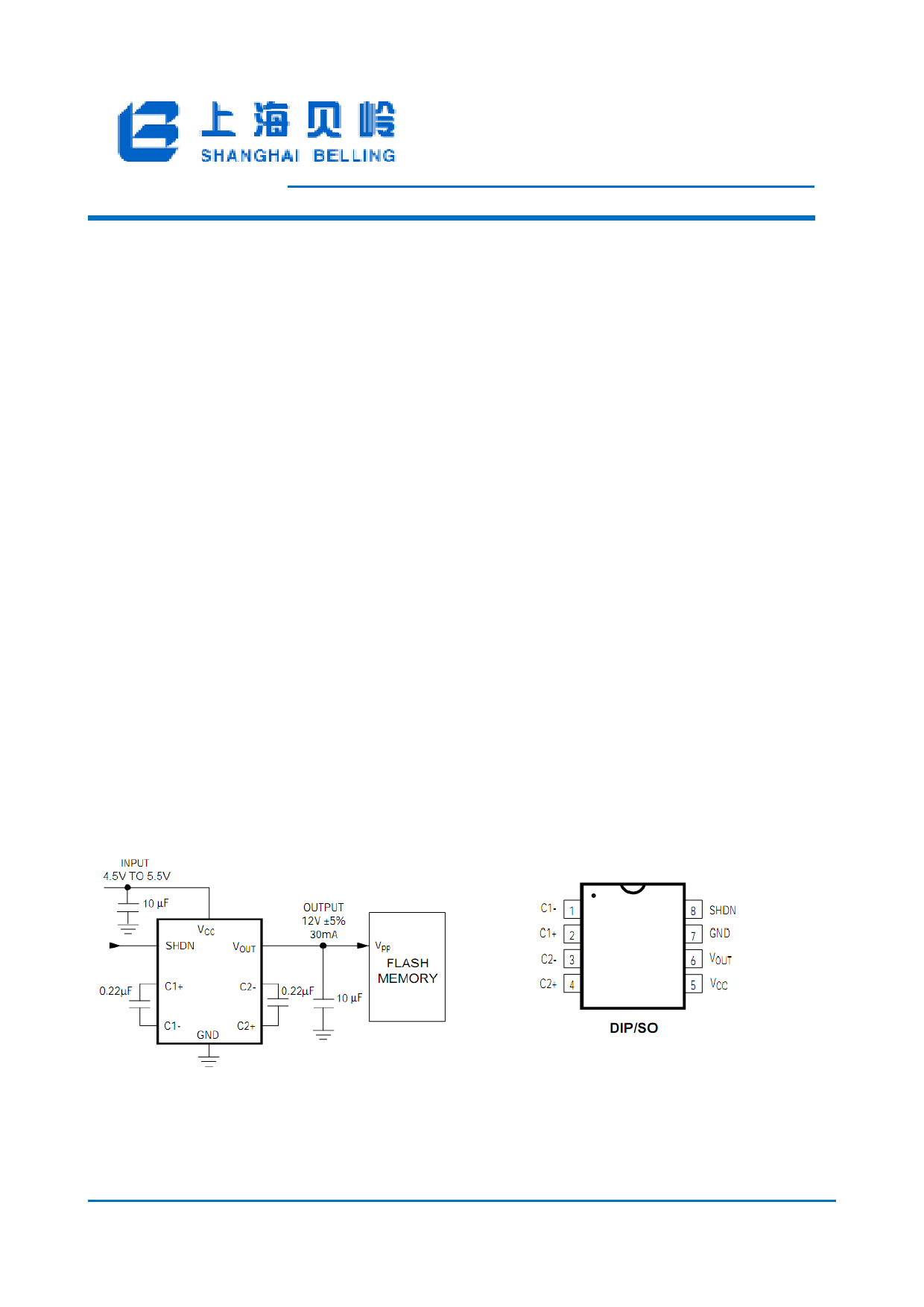
TYPICAL APPLICATION
BL8052
PIN OUT & MARKING
BL8052
www.belling.com.cn
1
1 page 
BL8052
DETAILED DESCRIPTION
BL8052 is a charge-pump IC. It can provide a 12V regulated output 30mA from voltage input as low as
4.75 without any inductors. It is useful for a wide range of applications and its performances makes it ideal for
flash memory programming supply.
Figure 1 is a simplified block diagram of BL8052. When the S1 switches are closed and the S2 switches
are open, capacitors C1 and C2 are charged up to VCC. And then the S1 switches are opened and the S2
switches are closed, capacitors C1 and C2 are connected in series between VCC and VOUT. A feedback
scheme adjusts the output voltage to 12V ±5%.
A good layout design is strongly recommended for noise reason. Very short connections to the
capacitors should be used for best performance. C3 and C4 must have low ESR in order to minimize the
output ripple. C1 and C2 should use ceramic or tantalum capacitors in the 0.22μF to 1.0μF range.
PACKAGE OUTLINE
Package
SOP8
Devices per reel
2500
Unit
mm
Package specification:
www.belling.com.cn
5
5 Page | ||
| Páginas | Total 5 Páginas | |
| PDF Descargar | [ Datasheet BL8052.PDF ] | |
Hoja de datos destacado
| Número de pieza | Descripción | Fabricantes |
| BL8051 | 60V Input / 5V Output Linear Regulator | BELLING |
| BL8052 | 30mA Flash Memory Programming Supply | BELLING |
| BL8053 | The charge pump mode 800mA LED flash driver IC | BELLING |
| Número de pieza | Descripción | Fabricantes |
| SLA6805M | High Voltage 3 phase Motor Driver IC. |
Sanken |
| SDC1742 | 12- and 14-Bit Hybrid Synchro / Resolver-to-Digital Converters. |
Analog Devices |
|
DataSheet.es es una pagina web que funciona como un repositorio de manuales o hoja de datos de muchos de los productos más populares, |
| DataSheet.es | 2020 | Privacy Policy | Contacto | Buscar |