|
|
|
PDF C8051F534A-IT Data sheet ( Hoja de datos )
| Número de pieza | C8051F534A-IT | |
| Descripción | 8/4/2 kB ISP Flash MCU | |
| Fabricantes | Silicon Laboratories | |
| Logotipo | ||
Hay una vista previa y un enlace de descarga de C8051F534A-IT (archivo pdf) en la parte inferior de esta página. Total 30 Páginas | ||
|
No Preview Available !
C8051F52x/F52xA/F53x/F53xA
8/4/2 kB ISP Flash MCU Family
Analog Peripherals
- 12-Bit ADC
• ±1 LSB INL; no missing codes
• Programmable throughput up to 200 ksps
• Up to 6/16 external inputs
• Data dependent windowed interrupt generator
• Built-in temperature sensor
- Comparator
• Programmable hysteresis and response time
• Configurable as wake-up or reset source
• Low current
- POR/Brownout Detector
- Voltage Reference—1.5 and 2.2 V (programma-
ble)
On-Chip Debug
- On-chip debug circuitry facilitates full-speed, non-
intrusive in-system debug (No emulator required)
- Provides breakpoints, single stepping
- Inspect/modify memory and registers
- Complete development kit
Supply Voltage 1.8 to 5.25 V
- Built-in LDO regulator
High-Speed 8051 µC Core
- Pipelined instruction architecture; executes 70% of
instructions in 1 or 2 system clocks
- Up to 25 MIPS throughput with
25 MHz system clock
- Expanded interrupt handler
Memory
- 8/4/2 kB Flash; In-system byte programmable in
512 byte sectors
- 256 bytes internal data RAM
Digital Peripherals
- 16/6 port I/O; push-pull or open-drain, 5 V tolerant
- Hardware SPI™, and UART serial port
- LIN 2.1 Controller (Master and Slave capable); no
crystal required
- Three general purpose 16-bit counter/timers
- Programmable 16-bit counter/timer array with three
capture/compare modules, WDT
Clock Sources
- Internal oscillators: 24.5 MHz ±0.5% accuracy sup-
ports UART and LIN-Master operation
- External oscillator: Crystal, RC, C, or Clock
(1 or 2 pin modes)
- Can switch between clock sources on-the-fly
Packages:
- 10-Pin DFN (3 x 3 mm)
- 20-pin QFN (4 x 4 mm)
- 20-pin TSSOP
Temperature Range: –40 to +125 °C
Rev. 1.0 4/09
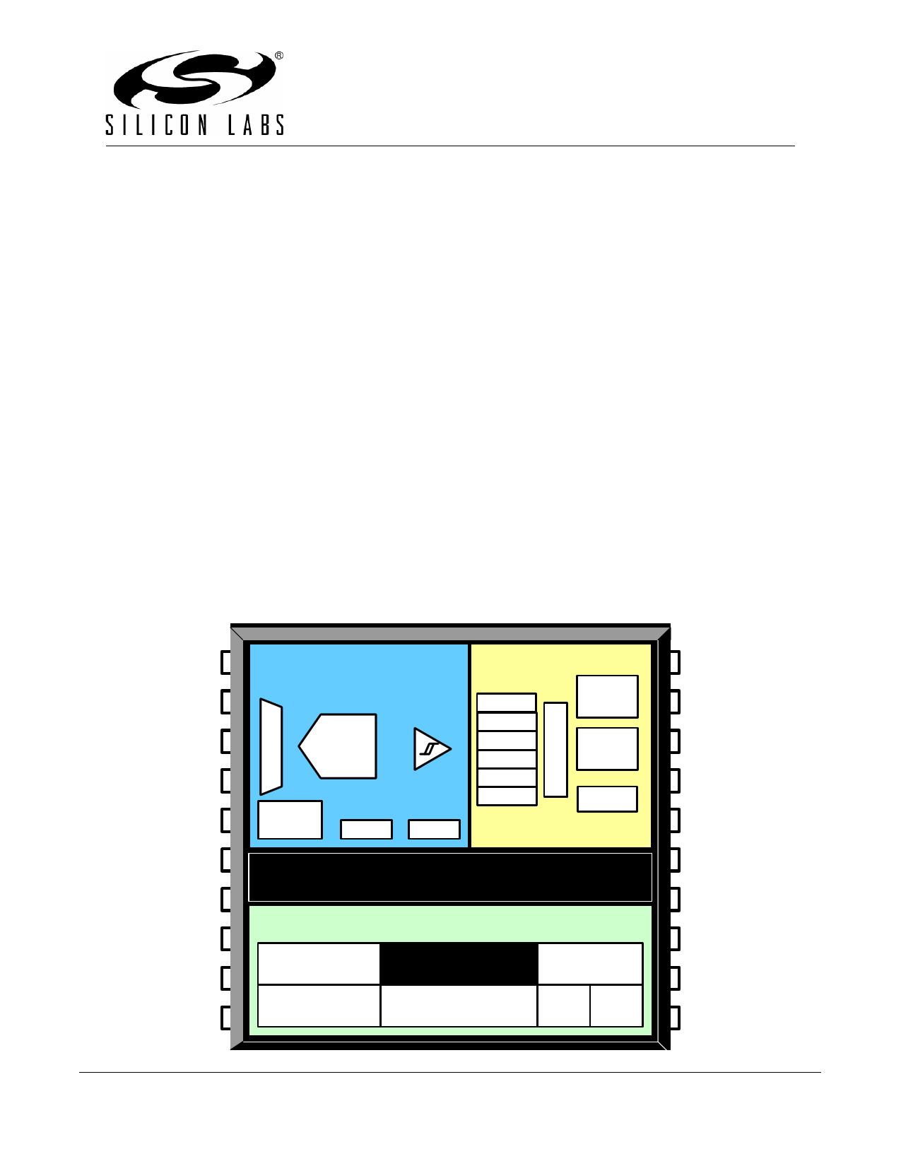
ANALOG
PERIPHERALS
A 12-bit
M
U
200 ksps
X ADC
+
-
TEMP
SENSOR
VOLTAGE
COMPARATOR
VREF VREG
DIGITAL I/O
UART
SPI
PCA
Timer 0
Timer 1
Timer 2
Port 0
Port 1
LIN
24.5 MHz High Precision (±0.5%) Internal Oscillator
HIGH-SPEED CONTROLLER CORE
8/4/2 kB
ISP FLASH
FLEXIBLE
INTERRUPTS
8051 CPU
(25 MIPS)
DEBUG
CIRCUITRY
256 B SRAM
POR WDT
Copyright © 2009 by Silicon Laboratories
C8051F52x/52xA/53x/53xA
1 page 
C8051F52x/F52xA/F53x/F53xA
14.2.4.External Capacitor Example................................................................... 144
14.3.System Clock Selection.................................................................................. 146
15. UART0.................................................................................................................... 147
15.1.Enhanced Baud Rate Generation................................................................... 148
15.2.Operational Modes ......................................................................................... 149
15.2.1.8-Bit UART ............................................................................................. 149
15.2.2.9-Bit UART ............................................................................................. 150
15.3.Multiprocessor Communications .................................................................... 150
16. Enhanced Serial Peripheral Interface (SPI0)...................................................... 155
16.1.Signal Descriptions......................................................................................... 156
16.1.1.Master Out, Slave In (MOSI).................................................................. 156
16.1.2.Master In, Slave Out (MISO).................................................................. 156
16.1.3.Serial Clock (SCK) ................................................................................. 156
16.1.4.Slave Select (NSS) ................................................................................ 156
16.2.SPI0 Master Mode Operation ......................................................................... 157
16.3.SPI0 Slave Mode Operation ........................................................................... 158
16.4.SPI0 Interrupt Sources ................................................................................... 159
16.5.Serial Clock Timing......................................................................................... 160
16.6.SPI Special Function Registers ...................................................................... 160
17. LIN (C8051F520/0A/3/3A/6/6A and C8051F530/0A/3/3A/6/6A)........................... 168
17.1. Software Interface with the LIN Peripheral .................................................. 169
17.2.LIN Interface Setup and Operation................................................................. 169
17.2.1.Mode Definition ...................................................................................... 169
17.2.2.Baud Rate Options: Manual or Autobaud .............................................. 169
17.2.3.Baud Rate Calculations - Manual Mode................................................. 169
17.2.4.Baud Rate Calculations—Automatic Mode ............................................ 171
17.3.LIN Master Mode Operation ........................................................................... 172
17.4.LIN Slave Mode Operation ............................................................................. 173
17.5.Sleep Mode and Wake-Up ............................................................................. 174
17.6.Error Detection and Handling ......................................................................... 175
17.7.LIN Registers.................................................................................................. 175
17.7.1.LIN Direct Access SFR Registers Definition .......................................... 175
17.7.2.LIN Indirect Access SFR Registers Definition........................................ 177
18. Timers.................................................................................................................... 185
18.1.Timer 0 and Timer 1 ....................................................................................... 185
18.1.1.Mode 0: 13-bit Counter/Timer ................................................................ 185
18.1.2.Mode 1: 16-bit Counter/Timer ................................................................ 187
18.1.3.Mode 2: 8-bit Counter/Timer with Auto-Reload...................................... 187
18.1.4.Mode 3: Two 8-bit Counter/Timers (Timer 0 Only)................................. 188
18.2.Timer 2 .......................................................................................................... 193
18.2.1.16-bit Timer with Auto-Reload................................................................ 193
18.2.2.8-bit Timers with Auto-Reload................................................................ 194
18.2.3.External Capture Mode .......................................................................... 195
19. Programmable Counter Array (PCA0) ................................................................ 198
19.1.PCA Counter/Timer ........................................................................................ 199
Rev. 1.0
5
5 Page 
C8051F52x/F52xA/F53x/F53xA
16. Enhanced Serial Peripheral Interface (SPI0)
Table 16.1. SPI Slave Timing Parameters ............................................................ 167
17. LIN (C8051F520/0A/3/3A/6/6A and C8051F530/0A/3/3A/6/6A)
Table 17.1. Baud-Rate Calculation Variable Ranges ............................................ 170
Table 17.2. Manual Baud Rate Parameters Examples ......................................... 171
Table 17.3. Autobaud Parameters Examples ........................................................ 172
Table 17.4. LIN Registers* (Indirectly Addressable) .............................................. 177
18. Timers
19. Programmable Counter Array (PCA0)
Table 19.1. PCA Timebase Input Options ............................................................. 199
Table 19.2. PCA0CPM Register Settings for PCA Capture/Compare Modules .... 200
Table 19.3. Watchdog Timer Timeout Intervals1 ................................................... 209
20. Device Specific Behavior
21. C2 Interface
Rev. 1.0
11
11 Page | ||
| Páginas | Total 30 Páginas | |
| PDF Descargar | [ Datasheet C8051F534A-IT.PDF ] | |
Hoja de datos destacado
| Número de pieza | Descripción | Fabricantes |
| C8051F534A-IM | 8/4/2 kB ISP Flash MCU | Silicon Laboratories |
| C8051F534A-IT | 8/4/2 kB ISP Flash MCU | Silicon Laboratories |
| Número de pieza | Descripción | Fabricantes |
| SLA6805M | High Voltage 3 phase Motor Driver IC. |
Sanken |
| SDC1742 | 12- and 14-Bit Hybrid Synchro / Resolver-to-Digital Converters. |
Analog Devices |
|
DataSheet.es es una pagina web que funciona como un repositorio de manuales o hoja de datos de muchos de los productos más populares, |
| DataSheet.es | 2020 | Privacy Policy | Contacto | Buscar |