|
|
|
PDF LD7921 Data sheet ( Hoja de datos )
| Número de pieza | LD7921 | |
| Descripción | Primary-Side PWM Power Switch | |
| Fabricantes | Leadtrend Technology | |
| Logotipo | ||
Hay una vista previa y un enlace de descarga de LD7921 (archivo pdf) en la parte inferior de esta página. Total 18 Páginas | ||
|
No Preview Available !
LD7921
02/02/2012
Primary-Side PWM Power Switch with CV/CC Operation
Ver. 00
General Description
The LD7921 integrated a 700V power MOSFET and a
primary-side feedback PWM controller with CV/CC
operation in a SOP-6/DIP-7 package. The LD7921 is
designed for low power adapter/charger and LED lighting
applications. It minimizes the components counts and is
available in tiny packages. Those make it an ideal design
for low cost applications.
The LD7921 provides constant voltage, constant current
(CV/CC) operation requiring neither photo-coupler nor
secondary control circuit. Also, the LD7921 features OTP
(Over Temperature Protection) and OVP (Over Voltage
Protection) to prevent the circuit from being damaged
under abnormal conditions.
Features
z Built-in 700V Power MOSFET
z Primary-side Feedback Control
z Constant Current Control
z Built-in Load Regulation Compensation
z Built-in Primary Winding Inductance Compensation
z Low Startup Current (<16μA)
z Current Mode Control with Cycle-by-Cycle Current
Limit
z Green Mode Control
z UVLO (Under Voltage Lockout)
z LEB (Leading-Edge Blanking) on CS Pin
z OVP (Over Voltage Protection) on Vcc
z OTP (Over Temperature Protection)
Applications
z AC-DC Adapter and Charger
z AC-DC LED Lighting
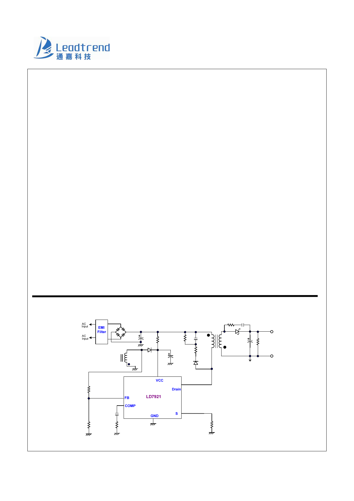
Typical Application
Leadtrend Technology Corporation
LD7921-DS-00 February 2012
1
www.leadtrend.com.tw
1 page 
LD7921
Absolute Maximum Ratings
Supply Voltage VCC,
Drain
COMP, FB, S
Maximum Junction Temperature
Peak Pulse drain current1, TC=25°C
Total Power Dissipation of SOP-6, Ta=25°C
Total Power Dissipation of DIP-7, Ta=25°C
Package thermal resistance (SOP-6), θJA
Package thermal resistance (DIP-7), θJA
Operating Ambient Temperature
Operating Junction Temperature
Storage Temperature Range
Lead temperature (Soldering, 10sec)
ESD Voltage Protection, Human Body Model (Exclusive Drain Pin)
ESD Voltage Protection, Machine Model (Exclusive Drain Pin)
1. Repetitive rating: Pulse width limited by maximum junction temperature
2. w/o heat-sink, under natural convection
-0.3 ~29V
-0.3~700V
-0.3 ~6V
150°C
1.0A
1.1W
1.2W
90°C /W2
80°C/W2
-40°C to 85°C
-40°C to 125°C
-65°C to 150°C
260°C
2.5 KV
250 V
Caution:
Stresses beyond the ratings specified in “Absolute Maximum Ratings” may cause permanent damage to the device. This is a stress only
rating and operation of the device at these or any other conditions above those indicated in the operational sections of this specification
is not implied.
Leadtrend Technology Corporation
LD7921-DS-00 February 2012
5
www.leadtrend.com.tw
5 Page 
LD7921
voltage clamp circuit to minimize the high frequency
ringing will achieve the best regulation. Fig. 17 shows the
desired drain voltage waveform in compare to Fig. 18 with
a large undershoot due to the leakage inductance induced
ring. This will cause error to the sample and inferior
performance to the output voltage regulation. A proper
selection for resistor RS, in series with the clamp diode,
may reduce any large undershoot, as shown in Fig. 19.
Fig. 15
Principle of CV Operation
In the DCM flyback converter, the output voltage can be
sensed by the auxiliary winding. LD7921 samples the
auxiliary winding on the primary-side to regulate the
output voltage, as shown in the Fig 16. The voltage
induced in the auxiliary winding is a reflection of the
secondary winding voltage while the MOSFET is in off
state. Via a resistor divider connected between the
auxiliary winding and FB pin, the auxiliary voltage is
sampled after the sample delay time and will be hold until
the next sampling. The sampled voltage is compared with
internal reference VREF (2.5V) and the error will be
amplified. The error amplifier output COMP reflects the
load condition and controls the duty cycle to regulate the
output voltage, thus constant output voltage can be
achieved. The output voltage is given as:
VOUT
=
2.5V(1 +
Ra
Rb
)(
Ns
Na
)
−
Vf
Where VF indicates the drop voltage of the output Diode,
Ra and Rb are values for top and bottom feedback
resistor, Ns and Na are the turns of transformer secondary
and auxiliary.
In case that the output voltage is sensed through the
auxiliary winding; the leakage inductance will induce
ringing to affect output regulation. Optimizing the drain
Leadtrend Technology Corporation
LD7921-DS-00 February 2012
11
www.leadtrend.com.tw
Fig.16
Fig.17
VDS
An undershoot
causes error to the
sample
Fig.18
11 Page | ||
| Páginas | Total 18 Páginas | |
| PDF Descargar | [ Datasheet LD7921.PDF ] | |
Hoja de datos destacado
| Número de pieza | Descripción | Fabricantes |
| LD7921 | Primary-Side PWM Power Switch | Leadtrend Technology |
| LD7922 | Primary-Side PWM Power Switch | Leadtrend Technology |
| Número de pieza | Descripción | Fabricantes |
| SLA6805M | High Voltage 3 phase Motor Driver IC. |
Sanken |
| SDC1742 | 12- and 14-Bit Hybrid Synchro / Resolver-to-Digital Converters. |
Analog Devices |
|
DataSheet.es es una pagina web que funciona como un repositorio de manuales o hoja de datos de muchos de los productos más populares, |
| DataSheet.es | 2020 | Privacy Policy | Contacto | Buscar |