|
|
PDF DM164 Data sheet ( Hoja de datos )
| Número de pieza | DM164 | |
| Descripción | 8x3-CHANNEL CONSTANT CURRENT LED DRIVER | |
| Fabricantes | SiTi | |
| Logotipo |  |
|
Hay una vista previa y un enlace de descarga de DM164 (archivo pdf) en la parte inferior de esta página. Total 28 Páginas | ||
|
No Preview Available !
DM164
Version
Issue Date
File Name
Total Pages
: A.001
: 2007/09/04
: SP-DM164-A.001.doc
: 28
8x3-CHANNEL CONSTANT CURRENT LED DRIVER
新竹市科學園區展業一路 9 號 7 樓之 1
SILICON TOUCH TECHNOLOGY INC.
9-7F-1, Prosperity Road I, Science Based Industrial Park,
Hsin-Chu, Taiwan 300, R.O.C.
Tel:886-3-5645656 Fax:886-3-5645626
1 page 
點晶科技股份有限公司
SILICON TOUCH TECHNOLOGY INC.
DM164
PIN NAME
FUNCTION
VDD1,VDD2 Power supply terminal.
VSS1~4 Ground terminal.
REXT_R
External resistor connected between REXT and GND
for driver current setting.
REXT_R controls outputs:
REXT_G
IOUT0, 3, 6, 9, 12, 15, 18, 21.
REXT_G controls outputs:
REXT_B
IOUT1, 4, 7, 10, 13, 16, 19, 22.
REXT_B controls outputs:
IOUT2, 5, 8, 11, 14, 17, 20, 23.
IOUT0~11 LED driver outputs.
IOUT12~23 LED driver outputs.
DIN
DOUT
DCK
DCKO
DCKPH
DOUTPH
LTH
LTHO
Serial input for grayscale PWM data and current
adjustment data.
Serial output for grayscale PWM data and current
adjustment data.
Synchronous clock input for serial data transfer. The
input data of DIN can be transferred at either the rising
edges of DCK or the falling edges of DCK depending
on the signal DCKPH.
Synchronous clock output for serial data transfer.
DCKO= DCK .
When DCKPH = L, input data is shifted in by rising
edge of DCK,
When DCKPH = H, input data is shifted in by falling
edge of DCK
When DOUTPH = H, DOUT is shifted out with half
DCK cycle delay
When DOUTPH = L, DOUT is shifted out without delay
Data latch input pin.
When DCKPH=L & LTH=H or DCKPH=H & LTH=L,
internal latches become transparent and PWM counter
value will be set to FFFF(h).
When DCKPH=L & LTH=L or DCKPH=H & LTH=H,
internal latches hold data.
Data latch output pin. LTHO= LTH
QFN48 / LQFP48
pin number
16,45
18,19,42,43
21
22
23
12,11,10,9,8,7,
6,5,4,3,2,1
36,35,34,33,32,31
30,29,28,27,26,25
48
37
47
38
14
15
46
39
GCK
Clock input for PWM operation. When DCKPH=L
(DCKPH=H), the internal PWM counter will count up
with rising (falling) edge of GCK.
44
8x3-CHANNEL CONSTANT CURRENT LED DRIVERS
Version:A.001
Page 4
5 Page 
點晶科技股份有限公司
SILICON TOUCH TECHNOLOGY INC.
DM164
Serial Data Interface
The DM164 includes a flexible data transfer interface. The data can be transferred from
DIN pin to the shift registers at either the rising edge of DCK or the falling edge of DCK
depending on the signal DCKPH. After all data are clocked in, a high level LTH signal can
transfer the serial data to the data latches (Level Sensitive). The serial data format can be
192-bit or 384-bit wide, depending on the operating mode of the device.
Operating Modes
The DM164 has two operating modes depending on the signal MSEL. Table 1 shows the
available operating modes. When MSEL = H, the device operates at the D&G mode. D&G
mode is used to set dot correction data and global brightness control data after IC power
up or any time. When MSEL = L, the device becomes GD mode. GD mode is used to set
grayscale PWM data after D&G mode.
MSEL
H
L
Table 1. Two Operating Modes
MODE
Dot Correction Data & Global Brightness Control
Data Input Mode (D&G mode)
Grayscale PWM Data Input Mode (GD mode)
SHIFT REGISTER
192-bit
384-bit
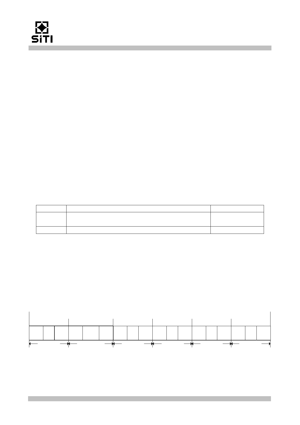
D&G Mode Data Format
At D&G mode, dot correction data of all channels and global brightness control data of
different colors are transferred into the chip at the same time. The complete dot correction
data format consists of 24 x 7-bit and the global brightness control data of three different
colors consists of 3 x 8-bit. The total shift registers width at D&G mode is 192-bit. All data
is clocked in with MSB first. Figure 1 shows the D&G mode data format.
MSB
191 185 184
31 30
24 23
16 15
87
LSB
0
IOUT23
IOUT23 IOUT22
DC6 ‧‧‧ DC0 DC6
‧‧‧
IOUT01 IOUT00
IOUT00
DC0 DC6 ‧‧‧ DC0
GB_R7
‧‧‧
GB_R0
GB_G7
‧‧‧
GB_G0
GB_B7
‧‧‧
GB_B0
IOUT23
IOUT22~IOUT01
IOUT00
GLOBAL_R
GLOBAL_G
GLOBAL_B
Figure 1. D&G Mode Data Format (D&G[191:0])
To operate the DM164 in D&G mode, MSEL must be set to high. The shift register width is
then set to 192-bit wide. The input data can be transferred at either the rising edge of DCK
8x3-CHANNEL CONSTANT CURRENT LED DRIVERS
Version:A.001
Page 10
11 Page | ||
| Páginas | Total 28 Páginas | |
| PDF Descargar | [ Datasheet DM164.PDF ] | |
Hoja de datos destacado
| Número de pieza | Descripción | Fabricantes |
| DM1601-7R | 50 Watt DC-DC Converters | Power-One |
| DM16116 | Display Module | Hantronix |
| DM1613 | 16 characters x 1 line Liquid Crystal Dot Matrix Display Module | Sanyo Semicon Device |
| DM161B | 16 characters x 1 line Liquid Crystal Dot Matrix Display Module | Sanyo Semicon Device |
| Número de pieza | Descripción | Fabricantes |
| SLA6805M | High Voltage 3 phase Motor Driver IC. |
Sanken |
| SDC1742 | 12- and 14-Bit Hybrid Synchro / Resolver-to-Digital Converters. |
Analog Devices |
|
DataSheet.es es una pagina web que funciona como un repositorio de manuales o hoja de datos de muchos de los productos más populares, |
| DataSheet.es | 2020 | Privacy Policy | Contacto | Buscar |
