|
|
|
PDF BM60054FV-C Data sheet ( Hoja de datos )
| Número de pieza | BM60054FV-C | |
| Descripción | 1ch Gate Driver Providing Galvanic Isolation | |
| Fabricantes | ROHM Semiconductor | |
| Logotipo | ||
Hay una vista previa y un enlace de descarga de BM60054FV-C (archivo pdf) en la parte inferior de esta página. Total 30 Páginas | ||
|
No Preview Available !
Datasheet
Gate Driver Providing Galvanic isolation Series
Isolation voltage 2500Vrms
1ch Gate Driver Providing Galvanic Isolation
BM60054FV-C
General Description
The BM60054FV-C is a gate driver with isolation voltage
2500Vrms, I/O delay time of 110ns, and a minimum input
pulse width of 90ns. Fault signal output function, ready
signal output function, under voltage lockout (UVLO)
function, short current protection (SCP) function, and
switching controller function are all built-in.
Features
■ Provides Galvanic Isolation
■ Fault Signal Output Function
■ Ready Signal Output Function
■ Under Voltage Lockout Function
■ Short Circuit Protection Function
■ Soft Turn-Off Function for Short Circuit Protection
(Adjustable Turn-OFF time)
■ Thermal Protection Function
■ Active Miller Clamping
■ Switching Controller Function
■ Output State Feedback Function
■ UL1577 Recognized:File No. E356010
■ AEC-Q100 Qualified(Note 1)
(Note 1:Grade1)
Key Specifications
Isolation Voltage:
Maximum Gate Drive Voltage:
I/O Delay Time:
Minimum Input Pulse Width:
2500Vrms
20V(Max)
110ns(Max)
90ns(Max)
Package
SSOP-B28W
W(Typ) x D(Typ) x H(Max)
9.2 mm x 10.4 mm x 2.4 mm
Applications
■ Driving IGBT Gate
■ Driving MOSFET Gate
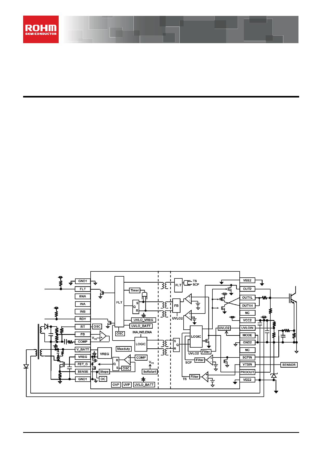
Typical Application Circuit
Figure 1. Typical Application Circuit
○Product structure:Silicon integrated circuit
.www.rohm.co.jp
© 2014 ROHM Co., Ltd. All rights reserved.
TSZ22111・14・001
○This product has no designed protection against radioactive rays
1/35
TSZ02201-0818ABH00080-1-2
10.Apr.2015 Rev.001
1 page 
BM60054FV-C
Electrical Characteristics
(Unless otherwise specified Ta=-40°C to +125°C, VBATT=4.0V to 32V, VCC2=UVLO to 20V, VEE2=-12V to 0V)
Parameter
Symbol
Min
Typ
Max Unit
Conditions
General
Main Power Supply
Circuit Current 1
IBATT1
1.1
1.6
2.1 mA V_BATT=4.0V
Main Power Supply
Circuit Current 2
IBATT2
0.8
1.3
1.8 mA V_BATT=12.0V
Main Power Supply
Circuit Current 3
IBATT3
0.8
1.3
1.8 mA V_BATT=32.0V
Output Side Circuit Current 1
Output Side Circuit Current 2
Output Side Circuit Current 3
Output Side Circuit Current 4
Output Side Circuit Current 5
ICC21
0.7
1.4
2.1 mA VCC2=14V, OUT1=L
ICC22
0.4
1.1
1.8 mA VCC2=14V, OUT1=H
ICC23
0.8
1.5
2.2 mA VCC2=18V, OUT1=L
ICC24
0.8
1.2
1.9 mA VCC2=18V, OUT1=H
ICC25
0.9
1.6
2.3
mA
VCC2=16V, VEE2=-8V,
OUT1=L
Output Side Circuit Current 6
ICC26
0.6
1.3
2.0
mA
VCC2=16V, VEE2=-8V,
OUT1=H
Switching Power Supply Controller
FET_G Output Voltage H1
VFETGH1
3.8
4.0
4.2
V
4.2V<V_BATT≤32V
IFET_G=0A(open)
FET_G Output Voltage H2
VFETGH2
-
V_BATT-0.2 V_BATT
V
V_BATT ≤ 4.2V
IFET_G =0A(open)
FET_G Output Voltage L
FET_G ON-Resistance
(Source-side)
VFETGL
RONGH
0
3
- 0.3 V IFET_G =0A(open)
6 12 Ω 10mA
FET_G ON-Resistance
(Sink-side)
RONGL
0.3
0.6
1.3 Ω 10mA
Oscillation Frequency
Soft-start Time
fSW 182 200 222 kHz RT=68kΩ
tSS -
- 50 ms
FB Pin Threshold Voltage
FB Pin Input Current
VFB 1.47 1.50 1.53 V
IFB -0.8
0
0.8 µA
COMP Pin Sink Current
COMP Pin Source Current
V_BATT UVLO ON Voltage
ICOMPSINK
ICOMPSOURCE
VUVLOBATTL
-160
40
3.20
-80
80
3.40
-40 µA
160 µA
3.60 V
V_BATT UVLO Hysteresis
Maximum ON DUTY
Over Voltage Detection Threshold
Under Voltage Detection
Threshold
Over-Current Detection Threshold
Protection Holding Time
Logic Block
VUVLOBATTHYS
DONMAX
VOVTH
VUVTH
VOCTH
tDCDCRLS
0.07
-
1.60
1.23
0.17
20
0.1
48
1.65
1.30
0.20
40
0.13
-
1.70
1.37
0.23
60
V
%
V
V
V
ms
Logic High Level Input Voltage VINH 2.0 - 5.5 V INA, INB, ENA
Logic Low Level Input Voltage VINL 0
- 0.8 V INA, INB, ENA
Logic Pull-Down Resistance
Logic Input Filtering Time
RIND
tINFIL
25
-
50 100 kΩ INA, INB, ENA
- 90 ns INA, INB
ENA Input Filtering Time
tENAFIL
-
0.5 0.8 µs ENA
MODE Low Level Input Voltage
VMODEL
0
-
0.3×VCC2
V MODE, relative to GND2
MODE High Level Input Voltage
VMODEH
0.7×VCC2
-
VCC2
V MODE,relative to GND2
www.rohm.co.jp
© 2014 ROHM Co., Ltd. All rights reserved.
TSZ22111・15・001
5/35
TSZ02201-0818ABH00080-1-2
10.Apr.2015 Rev.001
5 Page 
BM60054FV-C
1.45
1.25
1.05
0.85
0.65
0.45
-40
0 40 80 120
Ta [℃]
Figure 19. PROOUT ON-Resistance
(IPROOUT=40mA)
105
85
65
45
-40
0 40 80
Ta [℃]
Figure 20. Turn ON time
120
100
0.65
80
60 0.45
40
-40
0 40 80
Ta [℃]
Figure 21. Turn OFF time
120
0.25
-40
0 40 80
Ta [°C]
120
Figure 22. OUT2 ON-Resistance
(IOUT2=40mA)
www.rohm.co.jp
© 2014 ROHM Co., Ltd. All rights reserved.
TSZ22111・15・001
11/35
TSZ02201-0818ABH00080-1-2
10.Apr.2015 Rev.001
11 Page | ||
| Páginas | Total 30 Páginas | |
| PDF Descargar | [ Datasheet BM60054FV-C.PDF ] | |
Hoja de datos destacado
| Número de pieza | Descripción | Fabricantes |
| BM60054FV-C | 1ch Gate Driver Providing Galvanic Isolation | ROHM Semiconductor |
| Número de pieza | Descripción | Fabricantes |
| SLA6805M | High Voltage 3 phase Motor Driver IC. |
Sanken |
| SDC1742 | 12- and 14-Bit Hybrid Synchro / Resolver-to-Digital Converters. |
Analog Devices |
|
DataSheet.es es una pagina web que funciona como un repositorio de manuales o hoja de datos de muchos de los productos más populares, |
| DataSheet.es | 2020 | Privacy Policy | Contacto | Buscar |