|
|
|
PDF NCV6323 Data sheet ( Hoja de datos )
| Número de pieza | NCV6323 | |
| Descripción | 2A Synchronous Buck Converter | |
| Fabricantes | ON Semiconductor | |
| Logotipo | ||
Hay una vista previa y un enlace de descarga de NCV6323 (archivo pdf) en la parte inferior de esta página. Total 16 Páginas | ||
|
No Preview Available !
NCP6323, NCV6323
3 MHz, 2 A Synchronous
Buck Converter
High Efficiency, Low Ripple, Adjustable
Output Voltage
The NCP/NCV6323 is a synchronous buck converter which is
optimized to supply different sub systems of portable applications
powered by one cell Li−ion or three cell Alkaline/NiCd/NiMH
batteries. The devices are able to deliver up to 2 A on an external
adjustable voltage. Operation with 3 MHz switching frequency allows
employing small size inductor and capacitors. Input supply voltage
feedforward control is employed to deal with wide input voltage
range. Synchronous rectification offer improved system efficiency.
The NCP/NCV6323 is in a space saving, low profile 2.0 x 2.0 x
0.75 mm WDFN−8 package.
Features
• 2.5 V to 5.5 V Input Voltage Range
• External Adjustable Voltage
• Up to 2 A Output Current
• 3 MHz Switching Frequency
• Synchronous Rectification
• Enable Input
• Power Good Output Option
• Soft Start
• Over Current Protection
• Active Discharge When Disabled
• Thermal Shutdown Protection
• WDFN−8, 2 x 2 mm, 0.5 mm Pitch Package
• Maximum 0.8 mm Height for Super Thin Applications
• NCV Prefix for Automotive and Other Applications Requiring
Unique Site and Control Change Requirements; AEC−Q100
Qualified and PPAP Capable
• This is a Pb−Free Device
Typical Applications
• Cellular Phones, Smart Phones, and PDAs
• Portable Media Players
• Digital Still Cameras
• Wireless and DSL Modems
• USB Powered Devices
• Point of Load
• Game and Entertainment System
www.onsemi.com
1
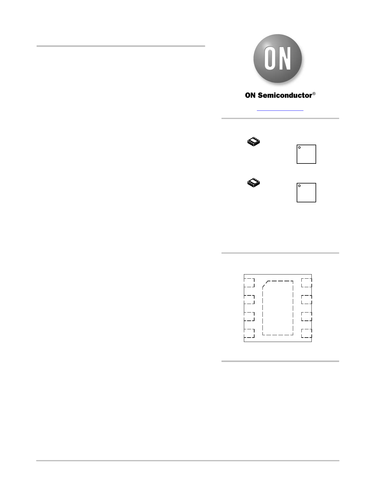
WDFN8
(NCV6323)
CASE 511BT
MARKING
DIAGRAMS
1
23 MG
G
1
WDFN8
(NCP6323)
CASE 511BE
1
NN MG
G
23/NN = Specific Device Code
M = Date Code
G = Pb−Free Package
(Note: Microdot may be in either location)
PGND 1
SW 2
AGND 3
FB 4
PINOUT
9
(Top View)
8 PVIN
7 AVIN
6 PG
5 EN
ORDERING INFORMATION
See detailed ordering, marking and shipping information on
page 2 of this data sheet.
© Semiconductor Components Industries, LLC, 2015
April, 2015 − Rev. 2
1
Publication Order Number:
NCV6323/D
1 page 
NCP6323, NCV6323
ELECTRICAL CHARACTERISTICS (VIN = 3.6 V, VOUT = 1.8 V, L = 1 mH, C = 10 mF, typical values are referenced to TJ = 25°C, Min
and Max values are referenced to TJ up to 125°C, unless other noted.)
Symbol
Characteristics
Test Conditions
Min Typ Max Unit
CONTROL LOGIC
VEN_H EN Input High Voltage
VEN_L EN Input Low Voltage
VEN_HYS EN Input Hysteresis
IEN_BIAS EN Input Bias Current
OUTPUT ACTIVE DISCHARGE
1.1 − − V
− − 0.4 V
− 270 − mV
0.1 1 mA
R_DIS Internal Output Discharge Resistance
from SW to PGND
75 500 700 W
THERMAL SHUTDOWN
TSD Thermal Shutdown Threshold
− 170 −
°C
TSD_HYS Thermal Shutdown Hysteresis
− 25 − °C
Product parametric performance is indicated in the Electrical Characteristics for the listed test conditions, unless otherwise noted. Product
performance may not be indicated by the Electrical Characteristics if operated under different conditions.
www.onsemi.com
5
5 Page 
NCP6323, NCV6323
APPLICATION INFORMATION
Output Filter Design Considerations
The output filter introduces a double pole in the system at
a frequency of
fLC
+
2
@
p
1
@ ǸL
@
C
(eq. 2)
The internal compensation network design of the
NCP/NCV6323 is optimized for the typical output filter
comprised of a 1.0 mH inductor and a 10 mF ceramic output
capacitor, which has a double pole frequency at about
50 kHz. Other possible output filter combinations may have
a double pole around 50 kHz to have optimum operation
with the typical feedback network. Normal selection range
of the inductor is from 0.47 mH to 4.7 mH, and normal
selection range of the output capacitor is from 4.7 mF to
22 mF.
Inductor Selection
The inductance of the inductor is determined by given
peak−to−peak ripple current IL_PP of approximately 20%
to 50% of the maximum output current IOUT_MAX for a
trade−off between transient response and output ripple. The
inductance corresponding to the given current ripple is
ǒVIN * VOUTǓ @ VOUT
L+
VIN @ fSW @ IL_PP
(eq. 3)
The selected inductor must have high enough saturation
current rating to be higher than the maximum peak current
that is
IL_PP
IL_MAX + IOUT_MAX ) 2
(eq. 4)
The inductor also needs to have high enough current
rating based on temperature rise concern. Low DCR is good
for efficiency improvement and temperature rise reduction.
Table 1 shows some recommended inductors for high power
applications and Table 2 shows some recommended
inductors for low power applications.
Table 1. LIST OF RECOMMENDED INDUCTORS FOR HIGH POWER APPLICATIONS
Manufacturer
Part Number
Case Size
(mm)
Rated Current (mA)
L (mH) (Inductance Drop)
MURATA
LQH44PN2R2MP0 4.0 x 4.0 x 1.8 2.2
2500 (−30%)
MURATA
LQH44PN1R0NP0 4.0 x 4.0 x 1.8 1.0
2950 (−30%)
MURATA
LQH32PNR47NNP0 3.0 x 2.5 x 1.7 0.47
3400 (−30%)
Structure
Wire Wound
Wire Wound
Wire Wound
Table 2. LIST OF RECOMMENDED INDUCTORS FOR LOW POWER APPLICATIONS
Manufacturer
Part Number
Case Size
(mm)
Rated Current (mA)
L (mH) (Inductance Drop)
MURATA
LQH44PN2R2MJ0 4.0 x 4.0 x 1.1 2.2
1320 (−30%)
MURATA
LQH44PN1R0NJ0 4.0 x 4.0 x 1.1 1.0
2000 (−30%)
TDK
VLS201612ET−2R2 2.0 x 1.6 x 1.2 2.2
1150 (−30%)
TDK
VLS201612ET−1R0 2.0 x 1.6 x 1.2 1.0
1650 (−30%)
Structure
Wire Wound
Wire Wound
Wire Wound
Wire Wound
Output Capacitor Selection
The output capacitor selection is determined by output
voltage ripple and load transient response requirement. For
a given peak−to−peak ripple current IL_PP in the inductor
of the output filter, the output voltage ripple across the
output capacitor is the sum of three ripple components as
below.
VOUT_PP [ VOUT_PP(C) ) VOUT_PP(ESR) ) VOUT_PP(ESL)
(eq. 5)
where VOUT_PP(C) is a ripple component by an equivalent
total capacitance of the output capacitors, VOUT_PP(ESR)
is a ripple component by an equivalent ESR of the output
capacitors, and VOUT_PP(ESL) is a ripple component by
an equivalent ESL of the output capacitors. In PWM
operation mode, the three ripple components can be
obtained by
IL_PP
VOUT_PP(C) + 8 @ C @ fSW
(eq. 6)
VOUT_PP(ESR) + IL_PP @ ESR
(eq. 7)
VOUT_PP(ESL)
+
ESL
ESL )
L
@
VIN
and the peak−to−peak ripple current is
ǒVIN * VOUTǓ @ VOUT
IL_PP +
VIN @ fSW @ L
(eq. 8)
(eq. 9)
www.onsemi.com
11
11 Page | ||
| Páginas | Total 16 Páginas | |
| PDF Descargar | [ Datasheet NCV6323.PDF ] | |
Hoja de datos destacado
| Número de pieza | Descripción | Fabricantes |
| NCV6323 | 2A Synchronous Buck Converter | ON Semiconductor |
| NCV6324 | 2A Synchronous Buck Converter | ON Semiconductor |
| Número de pieza | Descripción | Fabricantes |
| SLA6805M | High Voltage 3 phase Motor Driver IC. |
Sanken |
| SDC1742 | 12- and 14-Bit Hybrid Synchro / Resolver-to-Digital Converters. |
Analog Devices |
|
DataSheet.es es una pagina web que funciona como un repositorio de manuales o hoja de datos de muchos de los productos más populares, |
| DataSheet.es | 2020 | Privacy Policy | Contacto | Buscar |