|
|
|
PDF uP7701 Data sheet ( Hoja de datos )
| Número de pieza | uP7701 | |
| Descripción | 3A Ultra Low Dropout Linear Regulator | |
| Fabricantes | uPI Semiconductor | |
| Logotipo | ||
Hay una vista previa y un enlace de descarga de uP7701 (archivo pdf) en la parte inferior de esta página. Total 11 Páginas | ||
|
No Preview Available !
uP7701
3A Ultra Low Dropout Linear Regulator
General Description
Features
The uP7701 is a 3A ultra low dropout linear regulator
specifically designed for motherboard,notebook and graphic
card applications. This device works with dual supplies, a
control input for the control circuitry and a power input as
low as 1.0V for providing current to output. The uP7701
delivers high-current and ultra-low-drop output voltage as
low as 0.8V for applications where VOUT is very close to
VIN.
The uP7701 features comprehensive control and protection
functions: a power on reset (POR) circuit for monitoring
both control and power inputs for proper operation; an EN
input for enabling or disabling the device, a power OK with
time delay for indicating the output voltage status, a
foldback current limit function, and a thermal shutdown
function.
The uP7701 is available in PSOP-8 package with very low
thermal resistance.
Applications
Desktop PCs, Notebooks, and Workstations
Graphic Cards
Low Voltage Logic Supplies
Microprocessor and Chipset Supplies
Split Plane Microprocessor Supplies
Advanced Graphics Cards Supplies
SoundCards and Auxiliary Power Supplies
SMPS Post Regulators
Works with 1.0V~5.5V VIN
Adjustable Output Voltage, Down to 0.8V
1.5% Initial Accuracy
Excellent Line and Load Regulation
3A Guaranteed Output Current
300mV @ 3A Dropout Voltage
Very Low On-Resistance
100mΩ typical
VOUT Pull Low Resistance when Disabled
Low Reverse Leakage (Output to Input )
VOUT Power OK Signal
Fast Transient Response
Low External Component Count
Low Cost and Easy to Use
Enable Pin
Over Current and Over Temperature Protection
Ordering Information
Order Number
uP7701U8
Package Type
PSOP-8
Remark
Note: uPI products are compatible with the current IPC/
JEDEC J-STD-020 and RoHS requirements. They are 100%
matte tin (Sn) plating and suitable for use in SnPb or Pb-
free soldering processes.
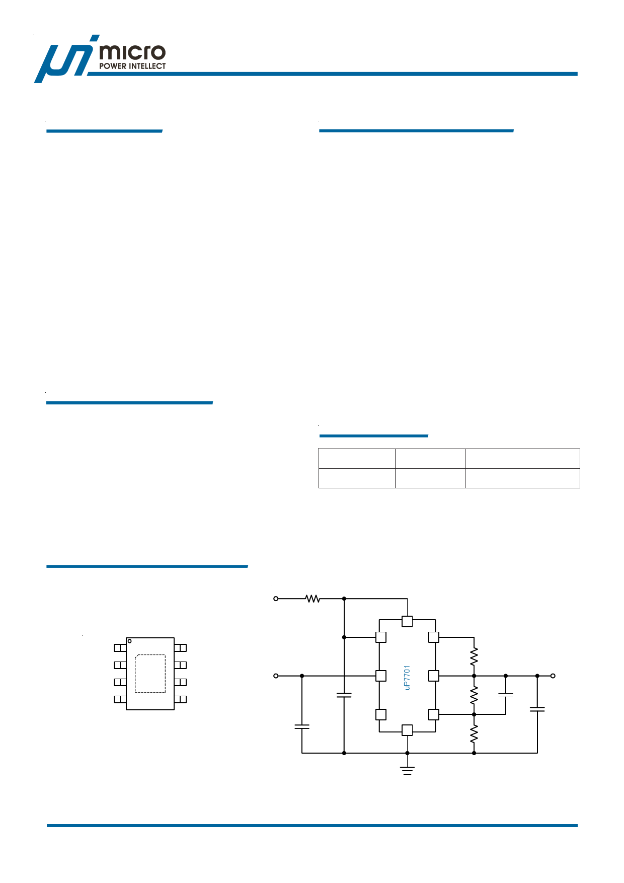
Pin Configuration & Typical Application Circuit
POK
EN
VIN
CNTL
18
27
GND
36
45
uP7701
GND
FB
VOUT
NC
5VCC
R4
10R
VIN
C1
1uF
C2
4.7uF
CNTL
EN
2
4
POK
1
VIN
3
VOUT
6
NC 5
FB
7
8
GND
R3
10K
R2
12.5K
R1
10K
VOUT
C4
option
C3
10uF
uPI Semiconductor Corp., http://www.upi-semi.com
Rev. 00, 2007, April
1
1 page 
uP7701
Electrical Characteristics
Parameter
Symbol
Feedback Voltage (VREFIN = VCNTL)
On Resistance
RDS(ON)
Dropout Voltage
VDROP
VOUT Pull Low Resistance
Enable
Test Conditions
IOUT = 100mA, VCNTL = VEN = 5.0V, VOUT = 1.6V
IOUT = 2A, VCNTL = VEN = 5.0V, VOUT = 1.6V, by design
IOUT = 3A, VCNTL = VEN = 5.0V, VOUT = 1.6V, by design
VCNTL = VIN = 5.0V, VEN = 0V, by design
Enable High Level
Disable Low Level
EN Source Current
EN Input Impedance
PWROK
VEN
VSD
IEN
ZEN
VEN = 0V, VCNTL = 5.0V
FB Power OK Threshold
Power OK Hysteresis
POK Delay Time
VPOKTH
VPOKHYS
Overcurrent Protection
OCP Threshold Level
Output Short Circuit
Current
IOCP
ISC
Thermal Protection
Thermal Shutdown
Temperature
TSD
Thermal Shutdown
Hysteresis
TSDHYS
IOUT = 0A, VCNTL = VIN = VEN = 5.0V, VOUT = VREF
IOUT = 0A, VCNTL = VIN = VEN = 5.0V, VOUT = VREF
From VOUT > 92% VNOM to POK rising
VCNTL = VIN = VEN = 5.0V, VOUT = VREF
VCNTL = VIN = VEN = 5.0V, VOUT = 0V
IOUT = 0A, VCNTL = VIN = VEN = 5.0V, VOUT = VREF
IOUT = 0A, VCNTL = VIN = VEN = 5.0V, VOUT = VREF
Min Typ Max Units
-- 100 120 mΩ
-- 200 240
mV
300 360
-- 90 --
Ω
-- -- 1.6 V
0.4 --
--
V
-- 12 20 uA
-- 65 -- KΩ
-- 92 --
%
-- 8 -- %
-- 1 -- ms
3.5 --
-- 100
--
--
A
mA
-- 170 --
-- 30 --
OC
OC
Note 1. Stresses listed as the above “Absolute Maximum Ratings” may cause permanent damage to the device.
These are for stress ratings. Functional operation of the device at these or any other conditions beyond those
indicated in the operational sections of the specifications is not implied. Exposure to absolute maximum
rating conditions for extended periods may remain possibility to affect device reliability.
Note 2. Devices are ESD sensitive. Handling precaution recommended.
Note 3. θJA is measured in the natural convection at TA = 25°C on a low effective thermal conductivity test board of
JEDEC 51-3 thermal measurement standard.
Note 4. The device is not guaranteed to function outside its operating conditions.
uPI Semiconductor Corp., http://www.upi-semi.com
Rev. 00, 2007, April
5
5 Page 
0.76 REF
1.27 REF
2.39 REF
uP7701
Application Information
4.80 - 5.00
2.29 BSC
1.27 BSC
0.32 - 0.52
Recommended Solder Pad Layout
1.45 - 1.60
0.20 BSC
0.41 - 0.89
0.18 - 0.25
1.75 MAX
3.81 BSC
0.10 - 0.25
Note
1.Package Outline Unit Description:
BSC: Basic. Represents theoretical exact dimension or dimension target
MIN: Minimum dimension specified.
MAX: Maximum dimension specified.
REF: Reference. Represents dimension for reference use only. This value is not a device specification.
TYP. Typical. Provided as a general value. This value is not a device specification.
2.Dimensions in Millimeters.
3.Drawing not to scale.
4.These dimensions no not include mold flash or protrusions. Mold flash or protrusions shell not exceed 0.15mm.
uPI Semiconductor Corp., http://www.upi-semi.com
Rev. 00, 2007, April
11
11 Page | ||
| Páginas | Total 11 Páginas | |
| PDF Descargar | [ Datasheet uP7701.PDF ] | |
Hoja de datos destacado
| Número de pieza | Descripción | Fabricantes |
| uP7701 | 3A Ultra Low Dropout Linear Regulator | uPI Semiconductor |
| uP7704 | 2A Ultra Low Dropout Linear Regulator | uPI Semiconductor |
| uP7706 | 3A Ultra Low Dropout Linear Regulator | uPI Semiconductor |
| Número de pieza | Descripción | Fabricantes |
| SLA6805M | High Voltage 3 phase Motor Driver IC. |
Sanken |
| SDC1742 | 12- and 14-Bit Hybrid Synchro / Resolver-to-Digital Converters. |
Analog Devices |
|
DataSheet.es es una pagina web que funciona como un repositorio de manuales o hoja de datos de muchos de los productos más populares, |
| DataSheet.es | 2020 | Privacy Policy | Contacto | Buscar |