|
|
|
PDF UT61L256 Data sheet ( Hoja de datos )
| Número de pieza | UT61L256 | |
| Descripción | 32K x 8 BIT HIGH SPEED LOW VCC CMOS SRAM | |
| Fabricantes | UTRON | |
| Logotipo | ||
Hay una vista previa y un enlace de descarga de UT61L256 (archivo pdf) en la parte inferior de esta página. Total 10 Páginas | ||
|
No Preview Available !
Rev. 1.3
UTRON
UT61L256
32K X 8 BIT HIGH SPEED LOW VCC CMOS SRAM
FEATURES
Fast access time : 8/10/12/15ns (max.)
Low operating power consumption:
60 mA (typical.)
Single 3.3V power supply
All inputs and outputs are TTL compatible
Fully static operation
Three state outputs
Package : 28-pin 300 mil SOJ
28-pin 8mm×13.4 mm STSOP
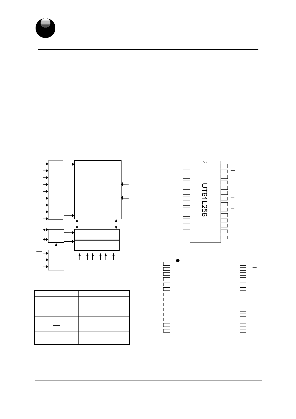
FUNCTIONAL BLOCK DIAGRAM
A4
A3
A14
A13
.
.A12 ROW
DECODER
A7
A6 .
A5
A8
I/O1
...
... I/O
CONTROL
I/O8
...
MEMORYARRAY
512 ROWS × 512 COLUMNS
. ..
COLUMNI/O
COLUMNDECODER
CE LOGIC
WE CONTROL
OE
A11 A9 A10 A2 A1 A0
VCC
VSS
PIN DESCRIPTION
SYMBOL
A0 - A14
I/O1 - I/O8
CE
WE
OE
VCC
VSS
DESCRIPTION
Address Inputs
Data Inputs/Outputs
Chip Enable Input
Write Enable Input
Output Enable Input
Power Supply
Ground
GENERAL DESCRIPTION
The UT61L256 is a 262,144-bit high speed CMOS
static random access memory organized as
32,768 words by 8 bits. It is fabricated using high
performance, high reliability CMOS technology.
The UT61L256 is designed for high-speed system
application. It is particularly suited for use in high
speed and high density system applications.
The UT61L256 operates from a signal 3.3V power
supply and all inputs and outputs are fully TTL
compatible
PIN CONFIGURATION
A14 1
A12 2
A7 3
A6 4
A5 5
A4 6
A3 7
A2 8
A1 9
A0 10
I/O1 11
I/O2 12
I/O3 13
Vss 14
28 Vcc
27 WE
26 A13
25 A8
24 A9
23 A11
22 OE
21 A10
20 CE
19 I/O8
18 I/O7
17 I/O6
16 I/O5
15 I/O4
SOJ
OE 1
A11 2
28
27
A9 3
26
A8 4
25
A13 5
WE 6
24
23
Vcc 7
22
A14 8 UT61L256 21
A12 9
A7 10
A6 11
20
19
18
A5 12
17
A4 13
16
A3 14
15
A10
CE
I/O8
I/O7
I/O6
I/O5
I/O4
Vss
I/O3
I/O2
I/O1
A0
A1
A2
STSOP
UTRON TECHNOLOGY INC.
1F, No. 11, R&D Rd. II, Science-Based Industrial Park, Hsinchu, Taiwan, R. O. C.
TEL: 886-3-5777882 FAX: 886-3-5777919
1
P80023
1 page 
Rev. 1.3
UTRON
UT61L256
32K X 8 BIT HIGH SPEED LOW VCC CMOS SRAM
WRITE CYCLE 1 ( WE Controlled) (1,2,3,5)
Address
CE
WE
DOUT
DIN
tAS
(4)
tWC
tAW
tCW
tWP
tWHZ High-Z
tWR
tOW
tDW tDH
Data Valid
(4)
WRITE CYCLE 2 ( CE Controlled) (1,2,5)
Address
CE
WE
DOUT
tWC
tAW
tAS tCW
tWP
tWHZ
(4)
DIN
tWR
High-Z
tDW tDH
Data Valid
Notes :
1. WE or CE must be HIGH during all address transitions.
2. A write occurs during the overlap of a low CE and a low WE .
3. During a WE controlled with write cycle with OE LOW, tWP must be greater than tWHZ+tDW to allow the drivers to turn off
and data to be placed on the bus.
4. During this period, I/O pins are in the output state, and input signals must not be applied.
5. If the CE LOW transition occurs simultaneously with or after WE LOW transition, the outputs remain
in a high impedance state.
6. tOW and tWHZ are specified with CL = 5pF. Transition is measured ±500mV from steady state.
UTRON TECHNOLOGY INC.
1F, No. 11, R&D Rd. II, Science-Based Industrial Park, Hsinchu, Taiwan, R. O. C.
TEL: 886-3-5777882 FAX: 886-3-5777919
5
P80023
5 Page | ||
| Páginas | Total 10 Páginas | |
| PDF Descargar | [ Datasheet UT61L256.PDF ] | |
Hoja de datos destacado
| Número de pieza | Descripción | Fabricantes |
| UT61L256 | 32K x 8 BIT HIGH SPEED LOW VCC CMOS SRAM | UTRON |
| Número de pieza | Descripción | Fabricantes |
| SLA6805M | High Voltage 3 phase Motor Driver IC. |
Sanken |
| SDC1742 | 12- and 14-Bit Hybrid Synchro / Resolver-to-Digital Converters. |
Analog Devices |
|
DataSheet.es es una pagina web que funciona como un repositorio de manuales o hoja de datos de muchos de los productos más populares, |
| DataSheet.es | 2020 | Privacy Policy | Contacto | Buscar |