|
|
PDF ICE3AS03LJG Data sheet ( Hoja de datos )
| Número de pieza | ICE3AS03LJG | |
| Descripción | Off-Line SMPS Current Mode Controller | |
| Fabricantes | Infineon Technologies | |
| Logotipo |  |
|
Hay una vista previa y un enlace de descarga de ICE3AS03LJG (archivo pdf) en la parte inferior de esta página. Total 25 Páginas | ||
|
No Preview Available !
Version 2.0, 3 Jul 2009
F3 PWM controller
ICE3AS03LJG
Off-Line SMPS Current Mode
Controller with integrated 500V
Startup Cell ( Latched and
frequency jitter Mode )
Power Management & Supply
Never stop thinking.
1 page 
F3 PWM controller
ICE3AS03LJG
Pin Configuration and Functionality
1 Pin Configuration and Functionality
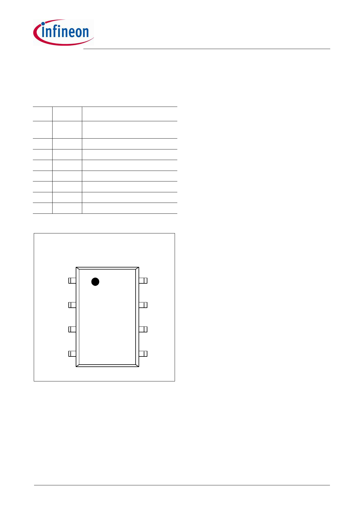
1.1 Pin Configuration with PG-DSO-8
1.2 Pin Functionality
Pin Symbol Function
1 BL extended Blanking and Latch off
enable
2 FB Feedback
3 CS Current Sense
4 Gate Gate driver output
5 HV High Voltage input
6 n.c. Not Connected
7 VCC Controller Supply Voltage
8 GND Controller Ground
BL (extended Blanking and Latch off enable)
The BL pin combines the functions of extendable
blanking time for entering the Auto Restart Protection
Mode and the external latch off enable. The extendable
blanking time function is to extend the built-in 20ms
blanking time by adding an external capacitor at BL to
ground. The external latch off enable function is an
external access to latch off the IC. It is triggered by
pulling down the BL pin to less than 0.33V.
FB (Feedback)
The information about the regulation is provided by the
FB Pin to the internal Protection Unit and to the internal
PWM-Comparator to control the duty cycle. The FB-
signal is the only control in case of light load at the
Active Burst Mode.
Package PG-DSO-8
BL 1
8 GND
CS (Current Sense)
The Current Sense pin senses the voltage developed
on the series resistor inserted in the source of the
Power MOSFET. If CS reaches the internal threshold
of the Current Limit Comparator, the Driver output is
immediately switched off. Furthermore, this current
information can be used to realize the Current Mode
operation through the PWM-Comparator where it
compares with FB signal.
FB 2
CS 3
Gate
4
Gate
7 VCC The Gate pin is the output of the internal driver stage
connected to the Gate of an external power MOSFET.
6 N.C. HV (High Voltage)
5 HV
The high voltage Pin is connected to the rectified DC
input voltage. It is the input for the integrated 500V
Startup cell.
Figure 1
Pin Configuration PG-DSO-8(top view)
VCC (Power supply)
The VCC pin is the positive supply of the IC. The
operating range is between 10.5V and 25V.
GND (Ground)
The GND pin is the ground of the controller.
Version 2.0
5
3 Jul 2009
5 Page 
F3 PWM controller
ICE3AS03LJG
Functional Description
decrease gradually and the duty ratio of the gate drive
increases gradually. The Soft Start will be finished in
10ms (tSoft-Start) after the IC is switched on. At the end of
the Soft Start period, the current sink is switched off.
VSoftS
VSOFTS32
tSoft-Start
In addition to Start-Up, Soft-Start is also activated at
each restart attempt during Auto Restart.
The Start-Up time tStart-Up before the converter output
voltage VOUT is settled, must be shorter than the Soft-
Start Phase tSoft-Start (see Figure 13).
By means of Soft-Start there is an effective
minimization of current and voltage stresses on the
external power MOSFET, the clamp circuit and the
output overshoot and it helps to prevent saturation of
the transformer during Start-Up.
Gate
Driver
3.5 PWM Section
0.75
t Oscillator
Duty Cycle
max
PWM Section
Clock
Frequency
t Jitter
Figure 12 Gate drive signal under Soft-Start Phase
Within the soft start period, the duty cycle is increasing
from zero to maximum gradually (see Figure 12).
VSoftS
VSOFTS32
tSoft-Start
Soft Start
Block
Soft Start
Comparator
PWM
Comparator
Current
Limiting
FF1
1S
Gate Driver
G8 R Q
&
G9
VFB
4.2V
VOUT
VOUT
tStart-Up
Figure 13 Start Up Phase
t
Figure 14 PWM Section Block
Gate
3.5.1
Oscillator
The oscillator generates a fixed frequency of 100kHz
with frequency jittering of ±4% (which is ±4kHz) at a
t jittering period of 4ms.
A capacitor, a current source and a current sink which
determine the frequency are integrated. The charging
and discharging current of the implemented oscillator
capacitor are internally trimmed, in order to achieve a
very accurate switching frequency. The ratio of
controlled charge to discharge current is adjusted to
t reach a maximum duty cycle limitation of Dmax=0.75.
Once the Soft Start period is over and when the IC goes
into normal operating mode, the switching frequency of
the clock is varied by the control signal from the Soft
Version 2.0
11
3 Jul 2009
11 Page | ||
| Páginas | Total 25 Páginas | |
| PDF Descargar | [ Datasheet ICE3AS03LJG.PDF ] | |
Hoja de datos destacado
| Número de pieza | Descripción | Fabricantes |
| ICE3AS03LJG | Off-Line SMPS Current Mode Controller | Infineon Technologies |
| Número de pieza | Descripción | Fabricantes |
| SLA6805M | High Voltage 3 phase Motor Driver IC. |
Sanken |
| SDC1742 | 12- and 14-Bit Hybrid Synchro / Resolver-to-Digital Converters. |
Analog Devices |
|
DataSheet.es es una pagina web que funciona como un repositorio de manuales o hoja de datos de muchos de los productos más populares, |
| DataSheet.es | 2020 | Privacy Policy | Contacto | Buscar |
