|
|
PDF D44TL1A0 Data sheet ( Hoja de datos )
| Número de pieza | D44TL1A0 | |
| Descripción | Digital Supervisor | |
| Fabricantes | Vicor | |
| Logotipo |  |
|
Hay una vista previa y un enlace de descarga de D44TL1A0 (archivo pdf) en la parte inferior de esta página. Total 25 Páginas | ||
|
No Preview Available !
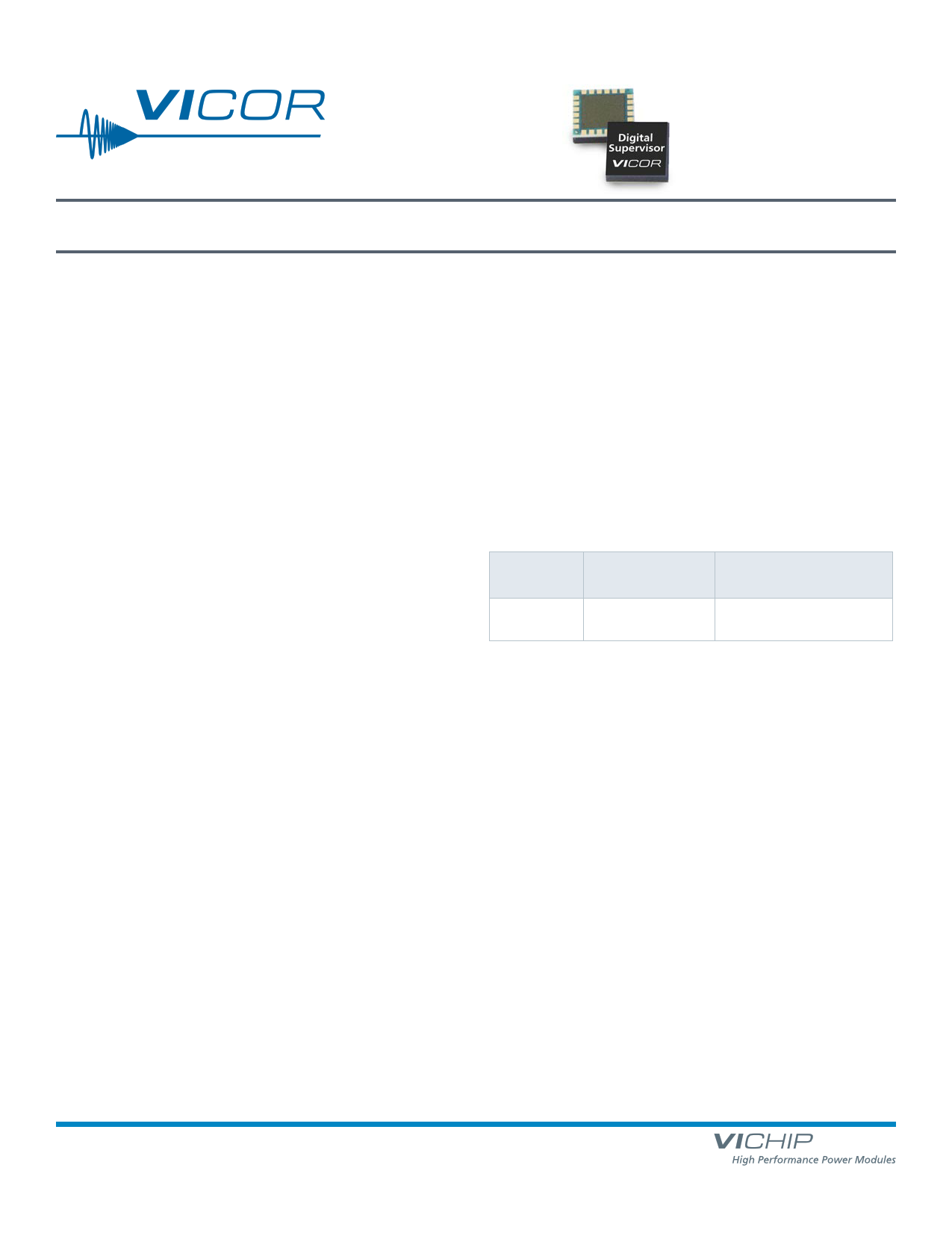
Digital Supervisor
D44TL1A0
For use with VI Chip® BCM Bus Converter Module
Features
• PMBus™ compatible host interface for enhanced
monitoring and control of ChiP BCM
Bus Converter Modules
• Interfaces with up to four BCMs through
dedicated UART interfaces via Vicor Digital
Isolators I13TL1A0 enabling secondary
referenced BCM control and telemetry
• OVP, OCP, OTP protection and monitoring
• 10 mm x 10 mm Land Grid Array (LGA) package
Typical Applications
• 380 VDC Power Distribution
• High End Computing Systems
• Automated Test Equipment
• Industrial Systems
• High Density Power Supplies
• Communications Systems
• Transportation
Product Description
The D44TL1A0 is a digital power system supervisor which
provides a communication interface between a host processor
and up to four ChiP BCM Bus Converter Modules. The
Supervisor communicates with a system controller via a
PMBus compatible interface. Acting as a communication
bridge, the Supervisor communicates with up to four BCM Bus
Converter Modules over isolated UART interfaces. Through the
D44TL1A0, the host processor can configure, set protection
limits, and monitor each BCM.
Standard Models
Part
Number
D44TL1A0
Package Type
LGA (10 x 10 mm)
Temperature
T-Grade (-40°C to 125°C)
BCM® Digital Supervisor
Page 1 of 25
Rev 1.2
12/2014
vicorpower.com
800 927.9474
1 page 
D44TL1A0
Absolute Maximum Ratings
The absolute maximum ratings below are stress ratings only. Operation at or beyond these maximum ratings can cause permanent damage to the device.
Parameter
VDD
IVDD
VDDB
RX4, RX3, RX2, RX1
TX4, TX3, TX2, TX1
SADDR, SSTOP
SCL, SDA
Comments
Min
-0.3
-0.3
-0.3
-0.3
-0.3
-0.3
Max
4.6
0.15
17.6
4.6
VVDD_IN + 0.5
3.6
5.5
Unit
V
A
V
V
V
V
V
Signal Characteristics
Specifications apply over the rated supply range (VDD or VDDB), unless otherwise noted; Boldface specifications apply over the temperature range of -40°C
≤ TINTERNAL ≤ 125°C (T-Grade); All other specifications are at TINTERNAL = 25ºC unless otherwise noted.
VDD Pin
• Regulated supply power input to the module, required when VDDB is not used to supply power to the device.
• Regulated output 3.3 V nominal output when supervisor is powered by VDDB.
• Intended to be used as low current supply for ancillary circuits.
SIGNAL TYPE
POWER
INPUT
POWER
OUTPUT
STATE
Regular
Operation
Startup
Regular
Operation
Transition
ATTRIBUTE
VDD Voltage input
VDD Current consumption
Inrush Current Peak
Turn on time
VDD Voltage output
VDD source Current
VDD Capacitance (External)
SYMBOL
CONDITIONS / NOTES
VVDD_IN
IVDD_IN
IVDD_ INR
tVDD_ON
VVDD_OUT
IVDD_OUT
CVDD_EXT
VVDD_IN Slew Rate = 1 V/µs
From VVDD_IN_MIN to PMBus™ active
MIN
3.0
3.23
TYP MAX UNIT
3.3 3.6 V
50 mA
2.5 A
1.5 ms
3.30 3.37 V
50 mA
1 µF
VDDB Pin
• Unregulated supply power input, required when VDD is not used as supply.
• This pin is a no connect pin if VDD pin is used to power the device.
SIGNAL TYPE
POWER
INPUT
STATE
Regular
Operation
Startup
ATTRIBUTE
VDDB Voltage
VDDB Current consumption
Inrush Current Peak
Turn on time
SYMBOL
CONDITIONS / NOTES
VVDDB
IVDDB
IVDDB_INR
tVDDB_ON
VVDDB Slew Rate = 1 V/µs
From VVDDB_MIN to PMBus active
MIN TYP MAX UNIT
3.6 16 V
50 mA
3.5 A
1.5 ms
SGND Pin
• Power supply return pin, and reference for all Digital Supervisor signal Input / Output.
BCM® Digital Supervisor
Page 5 of 25
Rev 1.2
12/2014
vicorpower.com
800 927.9474
5 Page 
D44TL1A0
PMBusTM Interface
Refer to “PMBus Power System Management Protocol
SpecificationRevision 1.2, Part I and II” for complete PMBus
specifications details visit http://pmbus.org.
Device Address
The PMBus address (SADDR Pin) should be set to one of a
predetermined 16 possible addresses shown in the table below using a
voltage divider from VDD to SGND.
The Digital Supervisor accepts only a fixed and persistent address and
does not support SMBus address resolution protocol. At initial
power-up, the Digital Supervisor will sample the address pin voltage,
and will hold this address until device power is removed.
ID
Slave
Address
1 1010 000b
2 1010 001b
3 1010 010b
4 1010 011b
5 1010 100b
6 1010 101b
7 1010 110b
8 1010 111b
9 1011 000b
10 1011 001b
11 1011 010b
12 1011 011b
13 1011 100b
14 1011 101b
15 1011 110b
16 1011 111b
HEX
50h
51h
52h
53h
54h
55h
56h
57h
58h
59h
5Ah
5Bh
5Ch
5Dh
5Eh
5Fh
Recommended
Resistor Divider (Ω)
R1 R2
13700
442
13300
1370
5760
1070
7320
2050
7150
2800
5230
2740
10700
7320
16200
14300
14300
16200
7320
10700
2740
5230
5360
13700
1690
6040
1070
5760
1370
13300
442 13700
BCM Enable Control Pin
The BCM EN Control pin input from host processor can be used to turn
the BCM powertrain on and off. The host will need to energize the
Digital Isolator channels of all used BCMs.
For a synchronous BCM startup, it is possible to connect all four Digital
Isolator pins (SER-IN-A) together. The input pin (SER-IN-A) to the
Digital Isolator requires at a minimum 2.5 V and N times 5 mA per N
number of channels driven for proper biasing. The output of each
Digital Isolator pin (SER-OUT-A) can then drive the respective BCM EN
pin. Refer to the Digital Isolator datasheet for more details.
The BCM EN pin has a higher priority level than the OPERATION
COMMAND (01h). The BCM powertrain will remain off if the BCM EN
pin is disabled.
Reported DATA Formats
The Digital Supervisor employs a direct data format where all reported
Digital Supervisor measurements are in Volts, Amperes, Degrees
Celsius, or Seconds. The host uses the following PMBus specification to
interpret received values metric prefixes. Note that the Coefficients
command is not supported:
X= (
1
m
) • (Y • 10-R - b)
Where:
X, is a “real world” value in units (A, V, °C, s)
Y, is a two’s complement integer received from the Digital Supervisor
m, b and R are two’s complement integers defined as follows:
Command
TON_DELAY
READ_VIN
READ_IIN
READ_VOUT
READ_IOUT
READ_TEMPERATURE_1
READ_POUT
MFR_VIN_MIN
MFR_VIN_MAX
MFR_VOUT_MIN
MFR_VOUT_MAX
MFR_IOUT_MAX
MFR_POUT_MAX
READ_K_FACTOR
READ_BCM_ROUT
Code
60h
88h
89h
8Bh
8Ch
8Dh
96h
A0h
A1h
A4h
A5h
A6h
A7h
D1h
D4h
m
1
1
1
1
1
1
1
1
1
1
1
1
1
65536
1
R
3
1
3
1
2
0
0
0
0
0
0
0
0
0
2
b
0
0
0
0
0
0
0
0
0
0
0
0
0
0
0
[1] Default READ Output Voltage returned when BCM unit is disabled = -300 V.
[2] Default READ Temperature returned when BCM unit is disabled = -273°C.
No special formatting is required when lowering the supervisory limits
and warnings.
BCM® Digital Supervisor
Page 11 of 25
Rev 1.2
12/2014
vicorpower.com
800 927.9474
11 Page | ||
| Páginas | Total 25 Páginas | |
| PDF Descargar | [ Datasheet D44TL1A0.PDF ] | |
Hoja de datos destacado
| Número de pieza | Descripción | Fabricantes |
| D44TL1A0 | Digital Supervisor | Vicor |
| Número de pieza | Descripción | Fabricantes |
| SLA6805M | High Voltage 3 phase Motor Driver IC. |
Sanken |
| SDC1742 | 12- and 14-Bit Hybrid Synchro / Resolver-to-Digital Converters. |
Analog Devices |
|
DataSheet.es es una pagina web que funciona como un repositorio de manuales o hoja de datos de muchos de los productos más populares, |
| DataSheet.es | 2020 | Privacy Policy | Contacto | Buscar |
