|
|
PDF FL7730MY Data sheet ( Hoja de datos )
| Número de pieza | FL7730MY | |
| Descripción | Single-Stage Primary-Side-Regulation PWM Controller | |
| Fabricantes | Fairchild Semiconductor | |
| Logotipo | ||
Hay una vista previa y un enlace de descarga de FL7730MY (archivo pdf) en la parte inferior de esta página. Total 13 Páginas | ||
|
No Preview Available !
February 2012
FL7730MY
Single-Stage Primary-Side-Regulation PWM Controller
for PFC and LED Dimmable Driving
Features
Compatible with Traditional TRIAC Control
(No need to change existing lamp infrastructure:
wall switch & wire)
Compatible with Non-Dimming Lamp Designs
Cost-Effective Solution without Input Bulk Capacitor
and Feedback Circuitry
Power Factor Correction (PFC)
Accurate Constant-Current (CC) Control,
Independent Online Voltage, Output Voltage,
Magnetizing Inductance Variation
Line Voltage Compensation for CC Control
Linear Frequency Control for Better Efficiency and
Simple Design
Open-LED Protection
Short-LED Protection
Cycle-by-Cycle Current Limiting
Over-Temperature Protection with Auto Restart
Low Startup Current: 20μA
Low Operating Current: 5mA
Frequency Hopping for Better EMI Performance
SOP-8 Package Available
Application Voltage Range: 80VAC ~ 308VAC
Description
This highly integrated PWM controller, FL7730MY,
provides several features to enhance the performance
of single-stage flyback converters. The proprietary
topology, TRUECURRENT™, enables the simplified
circuit design for LED lighting applications.
TRIAC dimming is smoothly managed by dimming
brightness control without flicker. By using single-stage
topology with primary-side regulation, an LED lighting
board can be implemented with few external
components and minimized cost. It does not require an
input bulk capacitor or feedback circuitry. To implement
good power factor and low total harmonic distortion,
constant on-time control is utilized with an external
capacitor connected to the COMI pin.
Precise constant-current control regulates accurate
output current versus changes in input voltage and
output voltage. The operating frequency is proportionally
changed by the output voltage to guarantee
Discontinuous Conduction Mode (DCM) operation with
higher efficiency and simpler design. The FL7730MY
provides protections such as open-LED, short-LED, and
over-temperature protections. Current-limit level is
automatically reduced to minimize output current and
protect external components in a short-LED condition.
The FL7730MY frequency-hopping function in the
oscillator improves EMI performance. The FL7730MY
controller is available in an 8-pin SOP package.
Applications
LED Lighting System
Ordering Information
Part Number
FL7730MY
Operating Temperature Range
-40°C to +125°C
Package
8-Lead, Small Outline Package
(SOP-8)
Packing Method
Tape & Reel
© 2011 Fairchild Semiconductor Corporation
FL7730MY • Rev. 1.0.3
www.fairchildsemi.com
1 page 
Electrical Characteristics
VDD=20V and TA=25°C unless otherwise specified.
Symbol
Parameter
VDD Section
VDD-ON Turn-On Threshold Voltage
VDD-OFF Turn-Off Threshold Voltage
IDD-OP Operating Current
IDD-ST
VOVP
Startup Current
VDD Over-Voltage-Protection
Gate Section
VOL
VOH
Isource
Isink
tr
tf
VCLAMP
Output Voltage Low
Output Voltage High
Peak Sourcing Current
Peak Sinking Current
Rising Time
Falling Time
Output Clamp Voltage
Oscillator Section
fMAX-CC
fMIN-CC
VSMAX-CC
VSMIN-CC
fHOPPING
fHOPPING
tON(MAX)
Maximum Frequency in CC
Minimum Frequency in CC
VS for Maximum Frequency in CC
VS for Minimum Frequency in CC
Frequency Hopping Range
Frequency Hopping Period
Maximum Turn-On Time
Current Sense Section
VRV
VCCR
Reference Voltage
EAI Voltage for Constant Current
Regulation
tLEB
tMIN
tPD
ttdis-BNK
ICOMI-BNK
Leading-Edge Blanking Time
Minimum On Time in CC
Propagation Delay to GATE
tDIS Blanking Time of VS
VS Current for COMI Blanking
Current-Error Amplifier Section
Gm Transconductance
ICOMI-SINK COMI Sink Current
ICOMI-SOURCE COMI Source Current
VCOMI-HGH COMI High Voltage
VCOMI-LOW COMI Low Voltage
Conditions
Min. Typ. Max. Units
Maximum Frequency,
CLOAD = 1nF
VDD = VDD-ON – 0.16V
14.5
6.75
3
22.0
16.0
7.75
4
2
23.5
17.5
8.75
5
20
25.0
V
V
mA
μA
V
VDD=20V,IGATE=-1mA
1.5 V
VDD=10V,IGATE=+1mA
5
V
VDD = 10 ~ 20V
60 mA
VDD = 10 ~ 20V
180 mA
CLOAD = 1nF
100 150 200 ns
CLOAD = 1nF
20 60 100 ns
12 15 18 V
f = fMAX -2kHz
f = fMIN +2kHz
60 65
21.0 23.5
2.25 2.35
0.55 0.85
±1.8 ±2.9
2
12 14
70 kHz
26.0 kHz
2.45 V
1.15 V
±4.0 kHz
ms
16 s
VCS = 0.44V
VCOMI = 0V
2.475
2.38
50
2.500
2.43
300
600
100
1.5
100
2.525
2.48
150
V
V
ns
ns
ns
s
A
VEAI=3V, VCOMI=5V
VEAI=2V, VCOMI=0V
VEAI=2V
VEAI=3V
85 mho
28 38 A
28 38 A
4.9 V
0.1 V
Continued on the following page…
© 2011 Fairchild Semiconductor Corporation
FL7730MY • Rev. 1.0.3
5
www.fairchildsemi.com
5 Page 
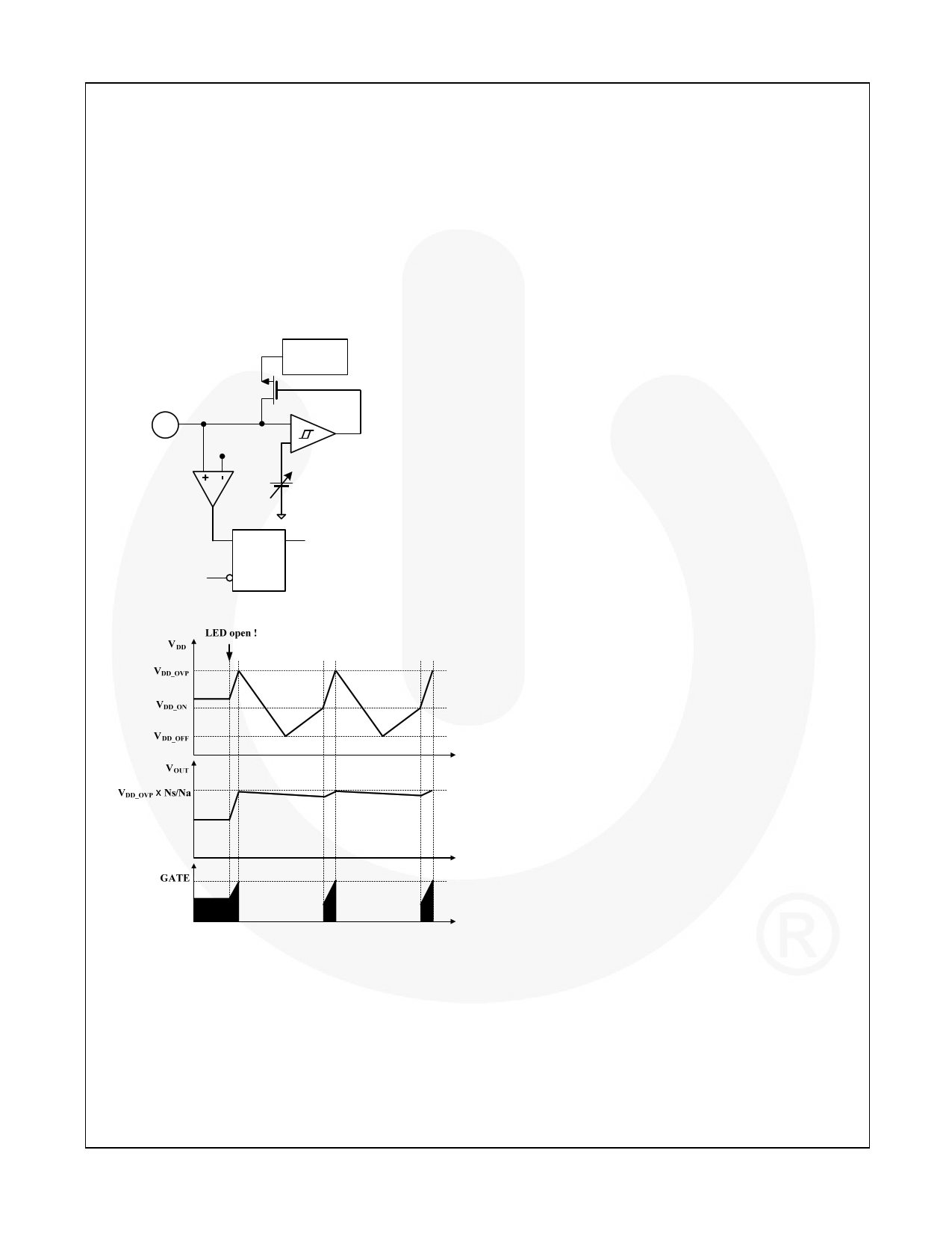
Open-LED Protection
FL7730 protects external components, such as diodes
and capacitors on the secondary side, in the open-LED
condition. During switch-off, the VDD capacitor is
charged up to the auxiliary winding voltage, which is
applied as the reflected output voltage. Because the VDD
voltage has output voltage information, the internal
voltage comparator on the VDD pin can trigger output
Over-Voltage Protection (OVP), as shown in Figure 24.
When at least one LED is open-circuited, output load
impedance becomes very high and output capacitor is
quickly charged up to VOVP x Ns / Na. Then switching is
shut down and VDD block goes into “Hiccup” Mode until
the open-LED condition is removed, shown in Figure 25.
Internal
Bias
VDD 4
VOVP
VDD good
+
-
S Q Shutdown gate driver
VDD good
R
Figure 24. Internal OVP Block
Under-Voltage Lockout (UVLO)
The turn-on and turn-off thresholds are fixed internally at
16V and 7.5V, respectively. During startup, the VDD
capacitor must be charged to 16V through the startup
resistor to enable the FL7730. The VDD capacitor
continues to supply VDD until power can be delivered
from the auxiliary winding of the main transformer. VDD
must not drop below 7.5V during this startup process.
This UVLO hysteresis window ensures that the VDD
capacitor is adequate to supply VDD during startup.
Over-Temperature Protection (OTP)
The built-in temperature-sensing circuit shuts down
PWM output if the junction temperature exceeds 150°C.
While PWM output is shut down, the VDD voltage
gradually drops to the UVLO voltage. Some of the
internal circuits are shut down and VDD gradually starts
increasing again. When VDD reaches 16V, all the
internal circuits start operating. If the junction
temperature is still higher than 140°C, the PWM
controller shuts down immediately.
Frequency Hopping
EMI reduction is accomplished by frequency hopping,
which spreads the energy over a wider frequency range
than the bandwidth measured by the EMI test
equipment. The internal frequency-hopping circuit
changes the switching frequency ±2.9kHz.
Figure 25. Waveforms in Open-LED Condition
© 2011 Fairchild Semiconductor Corporation
FL7730MY • Rev. 1.0.3
11
www.fairchildsemi.com
11 Page | ||
| Páginas | Total 13 Páginas | |
| PDF Descargar | [ Datasheet FL7730MY.PDF ] | |
Hoja de datos destacado
| Número de pieza | Descripción | Fabricantes |
| FL7730MY | Single-Stage Primary-Side-Regulation PWM Controller | Fairchild Semiconductor |
| Número de pieza | Descripción | Fabricantes |
| SLA6805M | High Voltage 3 phase Motor Driver IC. |
Sanken |
| SDC1742 | 12- and 14-Bit Hybrid Synchro / Resolver-to-Digital Converters. |
Analog Devices |
|
DataSheet.es es una pagina web que funciona como un repositorio de manuales o hoja de datos de muchos de los productos más populares, |
| DataSheet.es | 2020 | Privacy Policy | Contacto | Buscar |
