|
|
|
PDF IBIS4-1300 Data sheet ( Hoja de datos )
| Número de pieza | IBIS4-1300 | |
| Descripción | 1.3 MPxl Rolling Shutter CMOS Image Sensor | |
| Fabricantes | Cypress Semiconductor | |
| Logotipo | ||
Hay una vista previa y un enlace de descarga de IBIS4-1300 (archivo pdf) en la parte inferior de esta página. Total 30 Páginas | ||
|
No Preview Available !
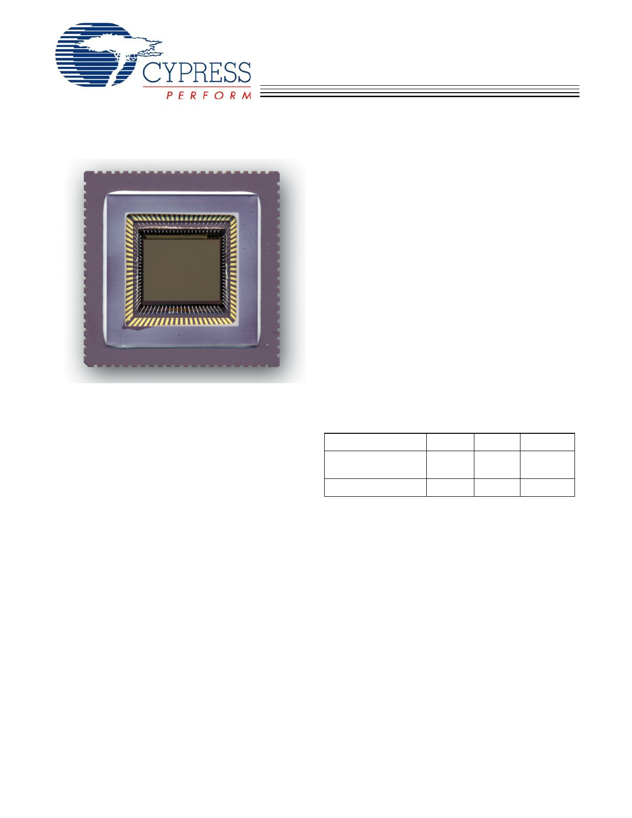
IBIS4-1300
1.3 MPxl Rolling Shutter CMOS Image
Sensor
Overview
The IBIS4-1300 is a digital CMOS active pixel image sensor
with SXGA format.
Due to a patented pixel configuration a 60% fill factor and 50%
quantum efficiency are obtained. This is combined with an
on-chip double sampling technique to cancel fixed pattern
noise.
Features
• SXGA resolution: 1280 x 1024 pixels
• High sensitivity 20 µV/e-
• High fill factor 60%
• Quantum efficiency > 50% between 500 and 700 nm.
• 20 noise electrons = 50 noise photons
• Dynamic range: 69 dB (2750:1) in single slope operation
• Extended dynamic range mode (80…100 dB) in double
slope integration
• On-chip 10 bit, 10 mega Samples/s ADC
• Programmable gain & offset output amplifier
• 4:1 sub sampling viewfinder mode (320x256 pixels)
• Electronic shutter
• 7 x 7 µm2 pixels
• Low fixed pattern noise (1% Vsat p/p)
• Low dark current: 344 pA/cm2
• (1055 electrons/s, 1 minute auto saturation)
• RGB or monochrome
• Digital (ADC) gamma correction
Part Number
Part Number
Package Glasslid RGB/B&W
CYII4SC1300AA-QSC LCC
S8612 RGBBayer
pattern
CYII4SM1300AA-QDC LCC
D263
B&W
Cypress Semiconductor Corporation
Document Number: 38-05707 Rev. *B
• 198 Champion Court • San Jose, CA 95134-1709 • 408-943-2600
Revised January 2, 2007
[+] Feedback
1 page 
IBIS4-1300
Image sensor core - focal plane array
Figure 1. shows the architecture of the image sensor core.
The core of the sensor is the pixel array with 1280 x 1024
(SXGA) active pixels.
The name 'active pixels' refers to the amplifying element in
each pixel. This type of pixels offer a high light sensitivity
combined with low temporal noise. The actual array size is
1286 x 1030 including the 6 dummy pixels in X and Y. Although
the dummy pixels fall outside the SXGA format, their
information can be used e.g. for color filter array interpolation.
Figure 2. Pixel selection - principle
X shift register
Next to the pixel array there are two Y shift registers, and one
X shift register with the column amplifiers. The shift registers
act as pointers to a certain row or column. The Y readout shift
register accesses the row (line) of pixels that is currently
readout. The X shift register selects a particular pixel of this
row. The second Y shift register is used to point at the row of
pixels that is reset. The delay between both Y row pointers
determines the integration time -thus realizing the electronic
shutter.
A clock and a synchronization pulse control the shift registers.
On every clock pulse, the pointer shifts one row/column
Table 1. optical & electrical characteristics
Pixel characteristics
Pixel structure
Photodiode
Pixel size
Resolution
Pixel rate with on-chip ADC
Frame rate with on-chip ADC
further. A sync pulse is used to reset and initialize the shift
registers to their first position.
The smart column amplifiers compensate the offset variations
between individual pixels. To do so, they need a specific pulse
pattern on specific control signals before the start of the row
readout.
Table 1. summarizes the optical and electrical characteristics
of the image sensor. Some specifications are influenced by the
output amplifier gain setting (e.g. temporal noise, conversion
factor,...). Therefore, all specifications are referred to an output
amplifier gain equal to 1.
3-transistor active pixel
High fill factor photodiode
7 x 7 µm2
1286 x 1030 pixels
SXGA plus 6 dummy rows & columns
Nominal 10 MHz (note 1) (note 2)
About 7 full frames/s at nominal speed
Document Number: 38-05707 Rev. *B
Page 5 of 37
[+] Feedback
5 Page 
IBIS4-1300
Table 2. Pins of the image sensor core
Digital controls
GND_AB
54
Power & ground
VDD_RESETL
VDD_RESETR
VDD_ARRAY
VDD
GND
59
79
55
11
34
53
77
10
33
52
78
Anti-blooming drain control voltage
• Default: connect to ground. The anti blooming is operational but
not maximal.
• Apply about 1 V DC for improved anti-blooming
Power supply for left reset line drivers apply 5 V DC (default) or about
4…4.5 V for dual slope mode
Power supply for right (default) reset line drivers 5 V DC
Power supply for the pixel array 5 V DC
Power supply of image sensor core & output amplifier 5 V DC
Ground of image sensor core & output amplifier
Output amplifier
The output amplifier stage is user-programmable for gain and
offset level. Gain and offset are controlled by 4-bit wide words.
Gain settings are on an exponential scale. Offset is controlled
by a 4-bit wide DAC, which selects the offset voltage between
2 reference voltages (Vhigh_dac & Vlow_dac) on a linear
scale.
Table 3. Summary of output amplifier specifications
Min.
Gain
1.2 (gain setting 0)
Output signal range
1V
Bandwidth
(40 pF load)
12 MHz
(gain setting 15)
Output slew rate
(40 pF load)
40 V/ µs
The offset setting is independent of the gain setting.
The gain setting is independent of amplifier bandwidth.
The amplifier is designed to match the specifications like the
output of the imager array. This signal has a data rate of 10
MHz and is located between 1.2 and 2.4 V. Table 3.
summarizes the specifications of the amplifier.
Typ
2.7 (setting 4)
22 MHz
(gain setting 0...8)
50 V/µs
Max
16 (setting 15)
4.5 V
33 MHz
(gain setting 0)
80 V/µs
The range of the output stage input is between 1 and 4 V. A
lowest gain the sensor outputs a signal in between 1.2 and 2.2
V, which fits into the input range of the amplifier. The range of
the output signal is between 1 and 4.5 V, dependent on the
gain and offset settings of the amplifier. This range should fit
to the input range of the ADC, external or internal. The
on-chip ADC range is between 2 and 4 V. A minimal gain
setting of "3" seems necessary for the internal ADC, and the
offset voltage should be set to the low-reference voltage of the
ADC.
Document Number: 38-05707 Rev. *B
Page 11 of 37
[+] Feedback
11 Page | ||
| Páginas | Total 30 Páginas | |
| PDF Descargar | [ Datasheet IBIS4-1300.PDF ] | |
Hoja de datos destacado
| Número de pieza | Descripción | Fabricantes |
| IBIS4-1300 | 1.3 MPxl Rolling Shutter CMOS Image Sensor | Cypress Semiconductor |
| Número de pieza | Descripción | Fabricantes |
| SLA6805M | High Voltage 3 phase Motor Driver IC. |
Sanken |
| SDC1742 | 12- and 14-Bit Hybrid Synchro / Resolver-to-Digital Converters. |
Analog Devices |
|
DataSheet.es es una pagina web que funciona como un repositorio de manuales o hoja de datos de muchos de los productos más populares, |
| DataSheet.es | 2020 | Privacy Policy | Contacto | Buscar |