|
|
|
PDF GAL16V8A-15QP Data sheet ( Hoja de datos )
| Número de pieza | GAL16V8A-15QP | |
| Descripción | HIGH PERFORMANCE E2CMOS PLD | |
| Fabricantes | Lattice Semiconductor | |
| Logotipo | ||
Hay una vista previa y un enlace de descarga de GAL16V8A-15QP (archivo pdf) en la parte inferior de esta página. Total 22 Páginas | ||
|
No Preview Available !
GAL16V8
High Performance E2CMOS PLD
Generic Array Logic™
Features
• HIGH PERFORMANCE E2CMOS® TECHNOLOGY
— 3.5 ns Maximum Propagation Delay
— Fmax = 250 MHz
— 3.0 ns Maximum from Clock Input to Data Output
— UltraMOS® Advanced CMOS Technology
• 50% to 75% REDUCTION IN POWER FROM BIPOLAR
— 75mA Typ Icc on Low Power Device
— 45mA Typ Icc on Quarter Power Device
• ACTIVE PULL-UPS ON ALL PINS
• E2 CELL TECHNOLOGY
— Reconfigurable Logic
— Reprogrammable Cells
— 100% Tested/100% Yields
— High Speed Electrical Erasure (<100ms)
— 20 Year Data Retention
• EIGHT OUTPUT LOGIC MACROCELLS
— Maximum Flexibility for Complex Logic Designs
— Programmable Output Polarity
— Also Emulates 20-pin PAL® Devices with Full
Function/Fuse Map/Parametric Compatibility
• PRELOAD AND POWER-ON RESET OF ALL REGISTERS
— 100% Functional Testability
• APPLICATIONS INCLUDE:
— DMA Control
— State Machine Control
— High Speed Graphics Processing
— Standard Logic Speed Upgrade
• ELECTRONIC SIGNATURE FOR IDENTIFICATION
Description
The GAL16V8, at 3.5 ns maximum propagation delay time, com-
bines a high performance CMOS process with Electrically Eras-
able (E2) floating gate technology to provide the highest speed
performance available in the PLD market. High speed erase times
(<100ms) allow the devices to be reprogrammed quickly and ef-
ficiently.
The generic architecture provides maximum design flexibility by
allowing the Output Logic Macrocell (OLMC) to be configured by
the user. An important subset of the many architecture configura-
tions possible with the GAL16V8 are the PAL architectures listed
in the table of the macrocell description section. GAL16V8 devices
are capable of emulating any of these PAL architectures with full
function/fuse map/parametric compatibility.
Unique test circuitry and reprogrammable cells allow complete AC,
DC, and functional testing during manufacture. As a result, Lattice
Semiconductor delivers 100% field programmability and function-
ality of all GAL products. In addition, 100 erase/write cycles and
data retention in excess of 20 years are specified.
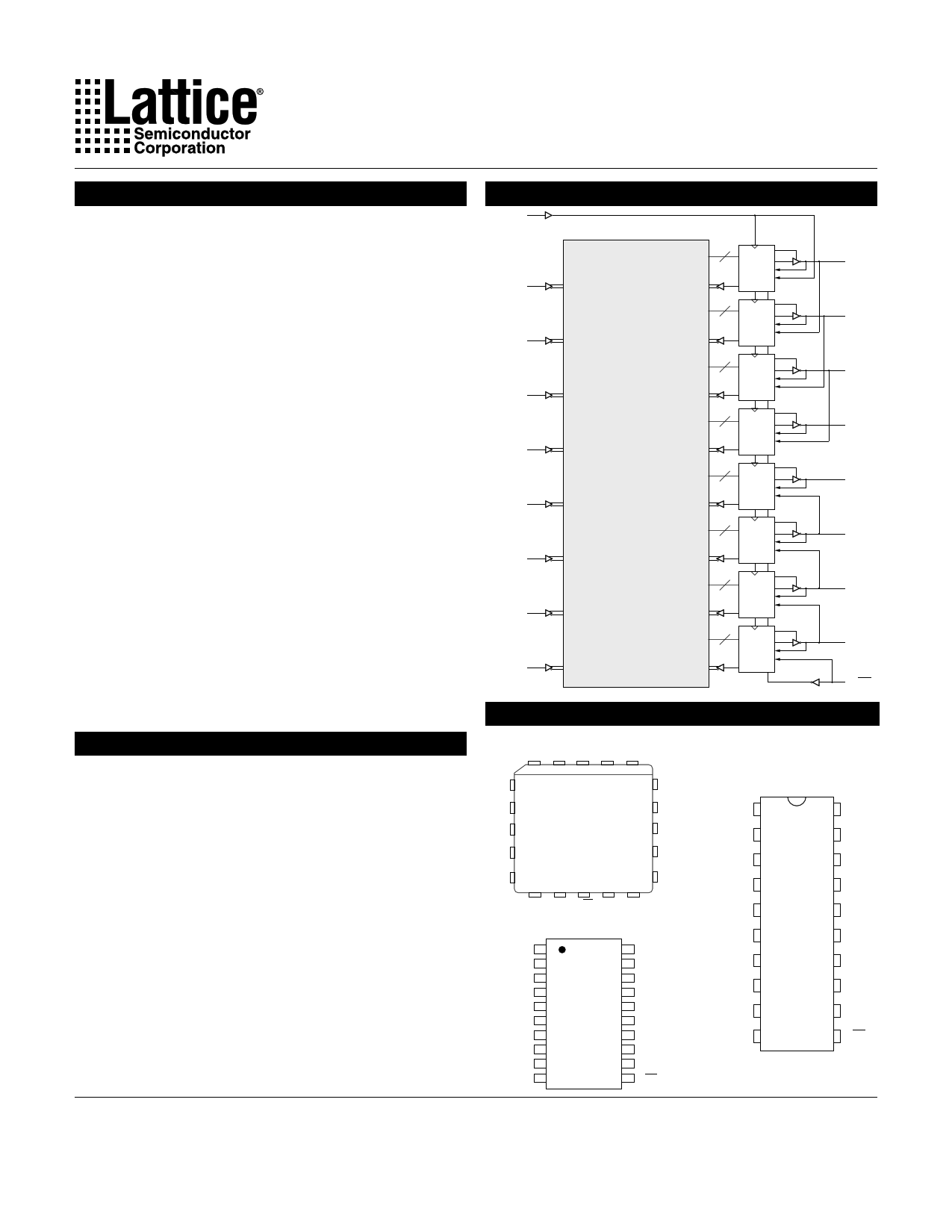
Functional Block Diagram
I/CLK
CLK
I
I
I
I
I
I
I
I
Pin Configuration
I
I4
PLCC
I I/CLK Vcc I/O/Q
2 20
18
I/O/Q
I GAL16V8 I/O/Q
I6
16 I/O/Q
Top View
I I/O/Q
I8
9
14 I/O/Q
11 13
I GND I/OE I/O/Q I/O/Q
I/CLK
I
I
I
I
I
I
I
I
GND
SOIC
1 20
GAL
5 16V8
Top 15
View
10 11
Vcc
I/O/Q
I/O/Q
I/O/Q
I/O/Q
I/O/Q
I/O/Q
I/O/Q
I/O/Q
I/OE
8 OLMC
8 OLMC
8 OLMC
8 OLMC
8 OLMC
8 OLMC
8 OLMC
8 OLMC
OE
I/O/Q
I/O/Q
I/O/Q
I/O/Q
I/O/Q
I/O/Q
I/O/Q
I/O/Q
I/OE
DIP
I/CLK
I
I
I
I
I
I
I
I
GND
1 20 Vcc
I/O/Q
GAL
16V8
5
I/O/Q
I/O/Q
I/O/Q
15 I/O/Q
I/O/Q
I/O/Q
I/O/Q
10 11 I/OE
Copyright © 2001 Lattice Semiconductor Corp. All brand or product names are trademarks or registered trademarks of their respective holders. The specifications and information herein are subject
to change without notice.
LATTICE SEMICONDUCTOR CORP., 5555 Northeast Moore Ct., Hillsboro, Oregon 97124, U.S.A.
Tel. (503) 268-8000; 1-800-LATTICE; FAX (503) 268-8556; http://www.latticesemi.com
May 2001
16v8_08
1
1 page 
Specifications GAL16V8
Registered Mode Logic Diagram
DIP & PLCC Package Pinouts
1
2128
0 4 8 12 16 20 24 28 PTD
0000
OLMC
0224
2
XOR-2048
AC1-2120
0256
0480
3
0512
0736
4
0768
0992
5
1024
1248
6
1280
1504
7
OLMC
XOR-2049
AC1-2121
OLMC
XOR-2050
AC1-2122
OLMC
XOR-2051
AC1-2123
OLMC
XOR-2052
AC1-2124
OLMC
XOR-2053
AC1-2125
1536
1760
8
OLMC
XOR-2054
AC1-2126
1792
2016
9
OLMC
XOR-2055
AC1-2127
2191
SYN-2192
AC0-2193
19
18
17
16
15
14
13
12
OE 11
5
5 Page 
Specifications GAL16V8D
AC Switching Characteristics
Over Recommended Operating Conditions
TEST
PARAMETER COND1.
DESCRIPTION
tpd A Input or I/O to Comb. Output
tco A Clock to Output Delay
tcf2 — Clock to Feedback Delay
tsu — Setup Time, Input or Feedback before Clock↑
th — Hold Time, Input or Feedback after Clock↑
A Maximum Clock Frequency with
External Feedback, 1/(tsu + tco)
COM
COM COM / IND
-3 -5 -7
UNITS
MIN. MAX. MIN. MAX. MIN. MAX.
1 3.5 1 5 1 7.5 ns
1 3 1 4 1 5 ns
— 2.5 — 3 — 3 ns
2.5 — 3 — 5 — ns
0 — 0 — 0 — ns
182 — 142.8 — 100 — MHz
fmax3
A Maximum Clock Frequency with
Internal Feedback, 1/(tsu + tcf)
200 — 166 — 125 — MHz
A Maximum Clock Frequency with
No Feedback
250 — 166 — 125 — MHz
twh — Clock Pulse Duration, High
2 4 — 3 4 — 4 — ns
twl — Clock Pulse Duration, Low
2 4 — 3 4 — 4 — ns
ten B Input or I/O to Output Enabled
B OE to Output Enabled
— 4.5 1 6 1 9 ns
— 4.5 1 6 1 6 ns
tdis C Input or I/O to Output Disabled
C OE to Output Disabled
— 4.5 1 5 1 9 ns
— 4.5 1 5 1 6 ns
1) Refer to Switching Test Conditions section.
2) Calculated from fmax with internal feedback. Refer to fmax Descriptions section.
3) Refer to fmax Descriptions section. Characterized but not 100% tested.
4) Characterized but not 100% tested.
Capacitance (TA = 25°C, f = 1.0 MHz)
SYMBOL
PARAMETER
CI Input Capacitance
CI/O I/O Capacitance
*Characterized but not 100% tested.
MAXIMUM*
8
8
UNITS
pF
pF
TEST CONDITIONS
VCC = 5.0V, VI = 2.0V
VCC = 5.0V, VI/O = 2.0V
11
11 Page | ||
| Páginas | Total 22 Páginas | |
| PDF Descargar | [ Datasheet GAL16V8A-15QP.PDF ] | |
Hoja de datos destacado
| Número de pieza | Descripción | Fabricantes |
| GAL16V8A-15QJ | HIGH PERFORMANCE E2CMOS PLD | Lattice Semiconductor |
| GAL16V8A-15QJI | HIGH PERFORMANCE E2CMOS PLD | Lattice Semiconductor |
| GAL16V8A-15QP | HIGH PERFORMANCE E2CMOS PLD | Lattice Semiconductor |
| GAL16V8A-15QPI | HIGH PERFORMANCE E2CMOS PLD | Lattice Semiconductor |
| Número de pieza | Descripción | Fabricantes |
| SLA6805M | High Voltage 3 phase Motor Driver IC. |
Sanken |
| SDC1742 | 12- and 14-Bit Hybrid Synchro / Resolver-to-Digital Converters. |
Analog Devices |
|
DataSheet.es es una pagina web que funciona como un repositorio de manuales o hoja de datos de muchos de los productos más populares, |
| DataSheet.es | 2020 | Privacy Policy | Contacto | Buscar |