|
|
|
PDF L6918AD Data sheet ( Hoja de datos )
| Número de pieza | L6918AD | |
| Descripción | 5 BIT PROGRAMMABLE MULTIPHASE CONTROLLER | |
| Fabricantes | STMicroelectronics | |
| Logotipo | ||
Hay una vista previa y un enlace de descarga de L6918AD (archivo pdf) en la parte inferior de esta página. Total 35 Páginas | ||
|
No Preview Available !
L6918 L6918A
5 BIT PROGRAMMABLE MULTIPHASE CONTROLLER
s OUTPUT CURRENT IN EXCESS OF 100A
s ULTRA FAST LOAD TRANSIENT RESPONSE
s REMOTE SENSE BUFFER
s INTEGRATED 2A GATE DRIVERS
s 5 BIT VID VOLTAGE POSITIONING, VRM 9.0
s 0.6% INTERNAL REFERENCE ACCURACY
s DIGITAL 2048 STEP SOFT-START
s OVP & OCP PROTECTIONS
s Rdson or Rsense CURRENT SENSING
s 1200KHz EFFECTIVE SWITCHING
FREQUENCY, EXTERNALLY ADJUSTABLE
s POWER GOOD OUTPUT AND INHIBIT
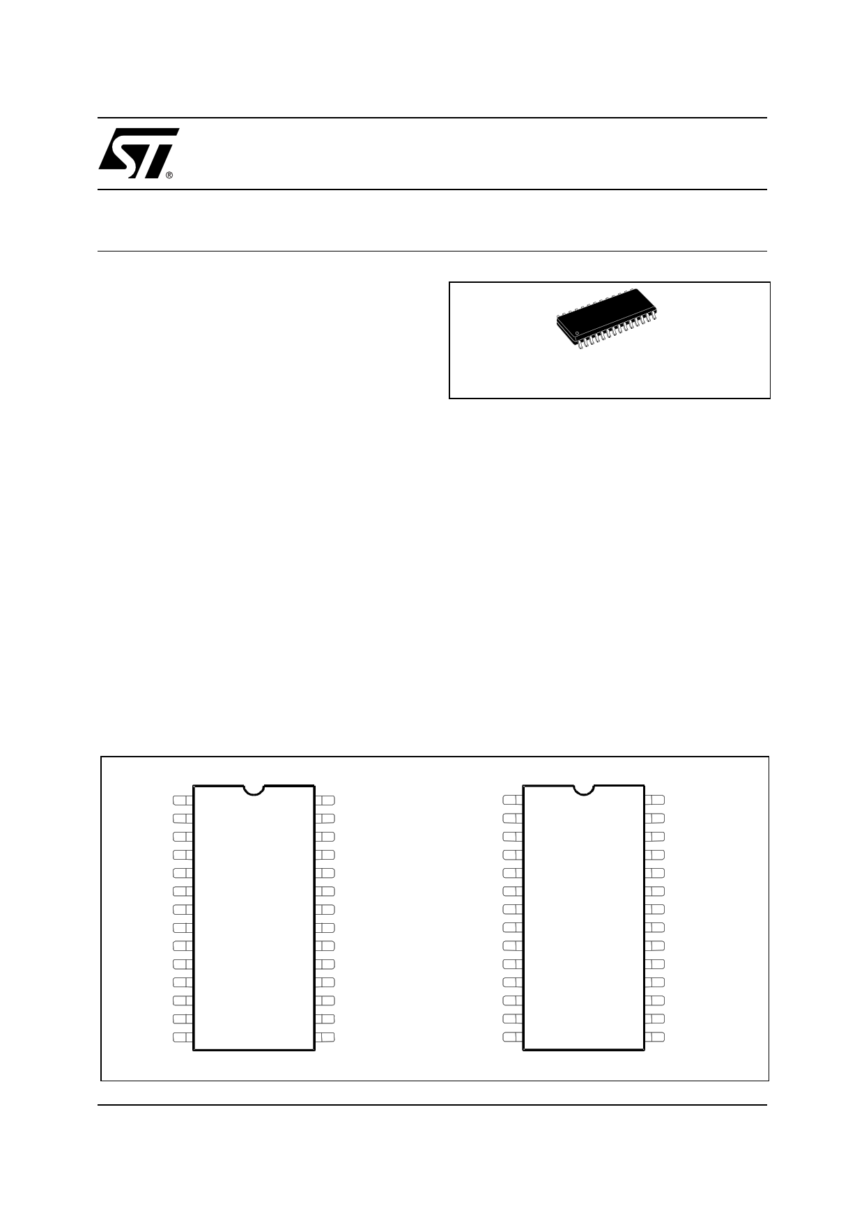
s PACKAGE: SO28
APPLICATIONS
s HIGH DENSITY DC-DC FOR SERVERS AND
WORKSTATIONS
s SUPPLY FOR HIGH CURRENT
MICROPROCESSORS
s DISTRIBUTED POWER
PIN CONNECTIONS
SO28
ORDERING NUMBERS: L6918D, L6918AD
L6918DTR, L6918ADTR
DESCRIPTION
L6918A is a master device that it has to be combined
with the L6918,slave, realizing a 4-phases topology,
interleaved. The device kit is specifically designed to
provide a high performance/high density DC/DC con-
version for high current microprocessors and distrib-
uted power. Each device implements a dual-phase
step-down controller with a 180° phase-shift between
each phase.
A precise 5-bit DAC allows adjusting the output volt-
age from 1.100V to 1.850V with 25mV binary steps.
The high peak current gate drives affords to have
high system switching frequency, typically of
1200KHz, and higher by external adjustement.
The device kit assure a fast protection against OVP,
UVP and OCP. An internal crowbar, by turning on the
low side mosfets, eliminates the need of external pro-
tection. In case of over-current, the system works in
Constant Current mode.
LGATE1
VCCDR
PHASE1
UGATE1
BOOT1
VCC
SGND
COMP
FB
VPROG_OUT
SYNC_OUT
SLAVE_OK
ISEN1
PGNDS1
1
2
3
4
5
6
7
8
9
10
11
12
13
14
October 2002
28 PGND
LGATE1
1
27 LGATE2
VCCDR
2
26 PHASE2
PHASE1
3
25 UGATE2
UGATE1
4
24 BOOT2
BOOT1
5
23 PGOOD
VCC
6
22 VID4
SGND
7
21 VID3
COMP
8
20 VID2
FB 9
19 VID1
VSEN
10
18 VID0
FBR 11
17 OSC / INH / FAULT
FBG
12
16 ISEN2
ISEN1
13
15 PGNDS2
PGNDS1
14
28 PGND
27 LGATE2
26 PHASE2
25 UGATE2
24 BOOT2
23 PGOOD
22 VPROG_IN
21 SYNC_IN
20 SLAVE_OK
19 SYNC / ADJ
18 SYNC_OUT
17 OSC / INH / FAULT
16 ISEN2
15 PGNDS2
1/35
1 page 
L6918 L6918A
L6918 (SLAVE) PIN FUNCTION
N. Name
Description
1 LGATE1 Channel 1 low side gate driver output.
2 VCCDR LS Mosfet driver supply. 5V or 12V buses can be used.
3 PHASE1 This pin is connected to the Source of the upper mosfet and provides the return path for the
high side driver of channel 1.
4 UGATE1 Channel 1 high side gate driver output.
5 BOOT1 Channel 1 bootstrap capacitor pin. This pin supplies the high side driver. Connect through a
capacitor to the PHASE1 pin and through a diode to Vcc (cathode vs. boot).
6
VCC
Device supply voltage. The operative supply voltage is 12V.
7
GND
All the internal references are referred to this pin. Connect it to the PCB signal ground.
8 COMP This pin is connected to the error amplifier output and is used to compensate the control
feedback loop.
9 FB This pin is connected to the error amplifier inverting input and is used to compensate the
voltage control feedback loop.
A current proportional to the sum of the current sensed in both channel is sourced from this pin
(50µA at full load, 70µA at the Over Current threshold). Connecting a resistor RFB between this
pin and VSEN pin allows programming the droop effect.
10 VSEN Connected to the output voltage it is able to manage Over & Under-voltage conditions and the
PGOOD signal. It is internally connected with the output of the Remote Sense Buffer for
Remote Sense of the regulated voltage.
If no Remote Sense is implemented, connect it directly to the regulated voltage in order to
manage OVP, UVP and PGOOD.
11
FBR
Remote sense buffer non-inverting input. It has to be connected to the positive side of the load
to perform a remote sense.
If no remote sense is implemented, connect directly to the output voltage (in this case connect
also the VSEN pin directly to the output regulated voltage).
12
FBG
Remote sense buffer inverting input. It has to be connected to the negative side of the load to
perform a remote sense.
Pull-down to ground if no remote sense is implemented.
13 ISEN1 Channel 1 current sense pin. The output current may be sensed across a sense resistor or
across the low-side mosfet RdsON. This pin has to be connected to the low-side mosfet drain or
to the sense resistor through a resistor Rg in order to program the current intervention for each
phase at 140% as follow:
IOCPx = 3----5R----µ-s--A-e---n--⋅-s--R-e----g-
Where 35µA is the current offset information relative to the Over Current condition (offset at
OC threshold minus offset at zero load).
The net connecting the pin to the sense point must be routed as close as possible to the
PGNDS1 net in order to couple in common mode any picked-up noise.
14 PGNDS1 Channel 1 Power Ground sense pin. The net connecting the pin to the sense point must be
routed as close as possible to the ISEN1 net in order to couple in common mode any picked-up
noise.
15 PGNDS2 Channel 2 Power Ground sense pin. The net connecting the pin to the sense point must be
routed as close as possible to the ISEN2 net in order to couple in common mode any picked-up
noise.
5/35
5 Page 
L6918 L6918A
– Clock Signal (SYNC_IN / SYNC_OUT pins): Unidirectional line.
A synchronization signal exits from the Master device through the SYNC_OUT pin with 90 deg phase-
shift and enters the Slave device through the SYNC_IN pin. The Slave device locks that signal
through an internal PLL for its regulation. An auxiliary synchronization signal exits from the Slave
through the SYNC_OUT.
– SLAVE_OK Bus (SLAVE_OK pins): Bi-directional line.
While the supply voltages are increasing, this line is hold to GND by all the devices. The Slave device
sets this line free (internally 5V pulled-up) when it is ready for the Soft-Start. After that this line is
freed, the Master device starts the Soft Start (for further details about Soft-Start, see the relevant sec-
tion).
During normal operation, the line is pulled low by the Slave device if an Over / Under voltage is de-
tected (See relevant section).
– PGOOD pins:
PGOOD pins are connected together and pulled-up. During Soft-Start, the master device hold down
this line while during normal regulation the slave device de-assert the line if PGOOD has been lost.
Connections between the devices are shown in figure 1.
OSCILLATOR
The devices have been designed in order to operate on each phase at the same switching frequency of the in-
ternal oscillator. So, input and output resulting frequencies are four times bigger.
The oscillator is present in all the devices. Since the Master oscillator sets the main frequency for the regulation,
the Slave oscillator gives an offset to the Slave's PLL. In this way the PLL is able to lock the synchronization
signal that enters from its SYNC_IN pin; it is able to recover up to ±15% offset in the synchronization signal fre-
quency. It is then necessary to program the switching frequency for all the devices involved in the multi-phase
conversion as follow.
The switching frequency is internally fixed to 300kHz. The internal oscillator generates the triangular waveform
for the PWM charging and discharging with a constant current an internal capacitor. The current delivered to the
oscillator is typically 25µA (Fsw = 300KHz) and may be varied using an external resistor (ROSC) connected be-
tween OSC pin and GND or Vcc. Since the OSC pin is maintained at fixed voltage (typ. 1.235V), the frequency
is varied proportionally to the current sunk (forced) from (into) the pin considering the internal gain of 12KHz/µA.
In particular connecting it to GND the frequency is increased (current is sunk from the pin), while connecting
ROSC to Vcc=12V the frequency is reduced (current is forced into the pin), according to the following relation-
ships:
ROSC vs. GND: fS = 300kHz + R-----O---1-S--.--C2---3(---K-7---Ω-----)- ⋅ 12 K---µ--H--A---z- = 300KHz + -R1---4-O--.--S8---2C----(-⋅--K-1---Ω-0---6-)-
ROSC vs. 12V: fS = 300kHz + R--1---2O----S-–---C-1--(--.-K2----3Ω---7---) ⋅ 12 K---µ--H--A---z- = 300KHz – -1-R--2--O-.--9-S--1--C--8--(--K⋅---1--Ω--0---)7-
Note that forcing a 25µA current into this pin, the device stops switching because no current is delivered to the
oscillator.
Figure 2 shows the frequency variation vs. the oscillator resistor ROSC considering the above reported relation-
ships.
11/35
11 Page | ||
| Páginas | Total 35 Páginas | |
| PDF Descargar | [ Datasheet L6918AD.PDF ] | |
Hoja de datos destacado
| Número de pieza | Descripción | Fabricantes |
| L6918A | 5 BIT PROGRAMMABLE MULTIPHASE CONTROLLER | STMicroelectronics |
| L6918AD | 5 BIT PROGRAMMABLE MULTIPHASE CONTROLLER | STMicroelectronics |
| L6918ADTR | 5 BIT PROGRAMMABLE MULTIPHASE CONTROLLER | STMicroelectronics |
| Número de pieza | Descripción | Fabricantes |
| SLA6805M | High Voltage 3 phase Motor Driver IC. |
Sanken |
| SDC1742 | 12- and 14-Bit Hybrid Synchro / Resolver-to-Digital Converters. |
Analog Devices |
|
DataSheet.es es una pagina web que funciona como un repositorio de manuales o hoja de datos de muchos de los productos más populares, |
| DataSheet.es | 2020 | Privacy Policy | Contacto | Buscar |