|
|
|
PDF L6910 Data sheet ( Hoja de datos )
| Número de pieza | L6910 | |
| Descripción | ADJUSTABLE STEP DOWN CONTROLLER WITH SYNCHRONOUS RECTIFICATION | |
| Fabricantes | STMicroelectronics | |
| Logotipo | ||
Hay una vista previa y un enlace de descarga de L6910 (archivo pdf) en la parte inferior de esta página. Total 29 Páginas | ||
|
No Preview Available !
L6910
L6910A
ADJUSTABLE STEP DOWN CONTROLLER
WITH SYNCHRONOUS RECTIFICATION
1 FEATURES
■ OPERATING SUPPLY VOLTAGE FROM 5V
TO 12V BUSES
■ UP TO 1.3A GATE CURRENT CAPABILITY
■ ADJUSTABLE OUTPUT VOLTAGE
■ N-INVERTING E/A INPUT AVAILABLE
■ 0.9V ±1.5% VOLTAGE REFERENCE
■ VOLTAGE MODE PWM CONTROL
■ VERY FAST LOAD TRANSIENT RESPONSE
■ 0% TO 100% DUTY CYCLE
■ POWER GOOD OUTPUT
■ OVERVOLTAGE PROTECTION
■ HICCUP OVERCURRENT PROTECTION
■ 200kHz INTERNAL OSCILLATOR
■ OSCILLATOR EXTERNALLY ADJUSTABLE
FROM 50kHz TO 1MHz
■ SOFT START AND INHIBIT
■ PACKAGES: SO-16 & HTSSOP16
2 APPLICATIONS
■ SUPPLY FOR MEMORIES AND TERMI-
NATIONS
■ COMPUTER ADD-ON CARDS
■ LOW VOLTAGE DISTRIBUTED DC-DC
■ MAG-AMP REPLACEMENT
3 DESCRIPTION
The device is a pwm controller for high performance
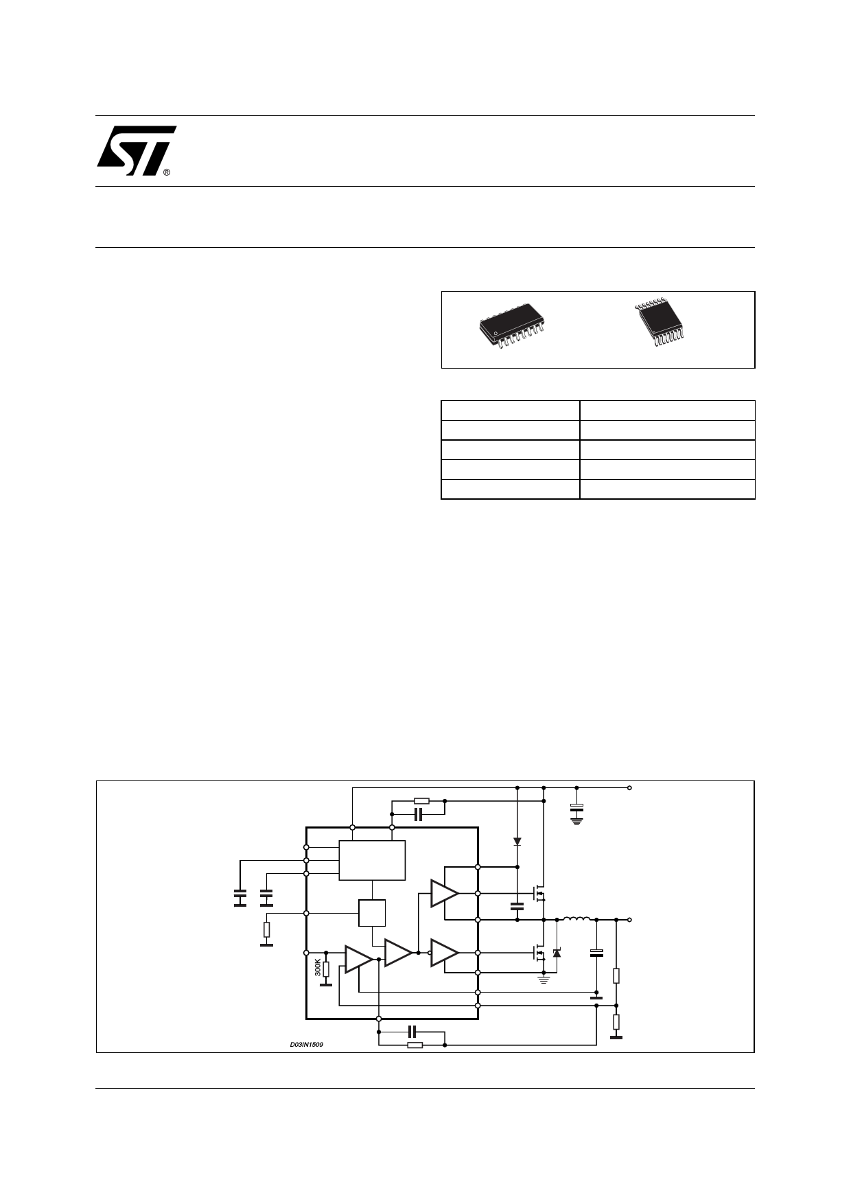
Figure 2. Block Diagram
PGOOD
VREF
SS
OSC
RT
EAREF
VCC OCSET
MONITOR
PROTECTION
& REF
OSC
E/A
+
-
PWM
-
+
May 2005
D03IN1509
COMP
Figure 1. Packages
SO-16 (Narrow)
HTSSOP16 (Exposed Pad)
Table 1. Order Codes
Part Number
Package
L6910
L6910TR
L6910A
SO-16
SO-16 in Tape & Reel
HTSSOP16
L6910ATR
HTSSOP16 in Tape & Reel
dc-dc conversion from 3.3V, 5V and 12V buses.
The output voltage is adjustable down to 0.9V;
higher voltages can be obtained with an external
voltage divider.
High peak current gate drivers provide for fast switch-
ing to the external power section, and the output
current can be in excess of 20A.
The device assures protections against load overcur-
rent and overvoltage. An internal crowbar is also pro-
vided turning on the low side mosfet as long as the
over-voltage is detected. In case of over-current de-
tection, the soft start capacitor is discharged and the
system works in HICCUP mode.
BOOT
UGATE
BOOT
LGATE
PGND
GND
VFB
Vin 5V to 12V
VO
Rev. 9
1/29
1 page 
L6910 - L6910A
4 DEVICE DESCRIPTION
The device is an integrated circuit realized in BCD technology. The controller provides complete con-
trol logic and protection for a high performance step-down DC-DC converter. It is designed to drive N
Channel Mosfets in a synchronous-rectified buck topology. The output voltage of the converter can be
precisely regulated down to 900mV with a maximum tolerance of ±1.5% when the internal reference is
used (simply connecting together EAREF and VREF pins). The device allows also using an external
reference (0.9V to 3V) for the regulation. The device provides voltage-mode control with fast transient
response. It includes a 200kHz free-running oscillator that is adjustable from 50kHz to 1MHz. The er-
ror amplifier features a 10MHz gain-bandwidth product and 10V/µs slew rate that permits to realize
high converter bandwidth for fast transient performance. The PWM duty cycle can range from 0% to
100%. The device protects against over-current conditions entering in HICCUP mode. The device
monitors the current by using the rDS(ON) of the upper MOSFET(s) that eliminates the need for a cur-
rent sensing resistor. The device is available in SO16 narrow package.
4.1 Oscillator
The switching frequency is internally fixed to 200kHz. The internal oscillator generates the triangular waveform
for the PWM charging and discharging with a constant current an internal capacitor. The current delivered to the
oscillator is typically 50µA (Fsw = 200KHz) and may be varied using an external resistor (RT) connected between
OSC pin and GND or VCC. Since the OSC pin is maintained at fixed voltage (typ. 1.235V), the frequency is var-
ied proportionally to the current sunk (forced) from (into) the pin.
In particular connecting RT vs. GND the frequency is increased (current is sunk from the pin), according to the
following relationship:
f O S C ,RT
=
200KHz + 4----.-9----4-----⋅---1---0----6-
RT(KΩ)
Connecting RT to VCC = 12V or to VCC = 5V the frequency is reduced (current is forced into the pin), according
to the following relationships:
fO S C ,RT
=
200KHz – -4---.--3---0---6-----⋅---1---0----7-
RT(KΩ)
VCC = 12V
fO S C ,RT
=
200KHz – -1---5-----⋅---1---0----6--
RT(KΩ)
VCC = 5V
Switching frequency variation vs. RT are repeated in Fig. 4.
Note that forcing a 50µA current into this pin, the device stops switching because no current is delivered to the
oscillator.
Figure 4.
10000
1000
100
10
10
RT to GND
RT to VCC=12V
RT to VCC=5V
100
Frequency [kHz]
1000
5/29
5 Page 
Figure 11. Asymptotic Bode Plot of Converter's Gain
dB Error Amplifier
L6910 - L6910A
R5/R3
Modulator Gain
ωΖ1
ωLC
ωΖ2
Compensation Network Gain
ωP1
ωP2
ωESR
Error Amplifier
Closed Loop Gain
ω
5 15A DEMO BOARD DESCRIPTION
The demo board shows the operation of the device in a general purpose application. This evaluation board al-
lows voltage adjustability from 0.9V to 5V through the switches S2-S5 according to the reported table when the
internal 0.9V reference is used (G1 closed). Output current in excess of 20A can be reached dependently on
the kind of mosfet used: up to three SO8 mosfet may be used for both High side and Low side switches. External
reference may be used for the regulation simply leaving open G1 and the switches S2-S5. The device may also
be disabled with the switch S1. The VCC input rail supplies the device while the power conversion starts from
the VIN input rail. The device is also able to operate with a single supply voltage; in this case the jumper G2 has
to be closed and a 5V to 12V input can be directly connected to the VIN input. The four layers demo board's
copper thickness is of 70µm in order to minimize conduction losses considering the high current that the circuit
is able to deliver.The PGOOD signal is used as a logic level and it's been pulled up to VIN because there's no
other appropriate voltage available on the demo board. In case of input voltage higher than 7V (PGOOD Pin
Maximum Absolute Rating) a 5V reference is required. Figure 12 shows the demo board's schematic circuit
Figure 12. 15A Demo Board Schematic
VIN
GNDIN
F1
G2
L1
R7 C14
C13
VCC
GNDCC
REFIN
GNDREFIN
+VREF
GNDREF
R6
C17
C16 G1
D1
VCC
C15
GND
EAREF
BOOT
15 12
7
8
OCSET
3
VREF
1
C12
UGATE
11
PHASE
10
LGATE
14
PGND
13
PGOOD
9
Q1-3
Q4-6
SS
4
C21
OSC
2
R1 5
6
COMP
C19
VFB
R5
R3
C20
S1 C18 R4
S2 R10
S3 R11
S4 SR12
S5 SR13
D03IN1513
C1-C3
L2
C4-
D2 11
R8
R9
VOUT
R2
GNDOUT
PWRGD
C22
VOUT S2 S3 S4 S5
0.9 Open Open Open Open
1.2 ON Open Open Open
1.5 Open ON Open Open
1.8 ON ON Open Open
2.5 Open Open ON Open
3.3 Open Open Open ON
5.0 Open Open ON ON
11/29
11 Page | ||
| Páginas | Total 29 Páginas | |
| PDF Descargar | [ Datasheet L6910.PDF ] | |
Hoja de datos destacado
| Número de pieza | Descripción | Fabricantes |
| L6910 | ADJUSTABLE STEP DOWN CONTROLLER WITH SYNCHRONOUS RECTIFICATION | STMicroelectronics |
| L6910A | ADJUSTABLE STEP DOWN CONTROLLER WITH SYNCHRONOUS RECTIFICATION | STMicroelectronics |
| L6910ATR | ADJUSTABLE STEP DOWN CONTROLLER WITH SYNCHRONOUS RECTIFICATION | STMicroelectronics |
| L6910TR | ADJUSTABLE STEP DOWN CONTROLLER WITH SYNCHRONOUS RECTIFICATION | STMicroelectronics |
| Número de pieza | Descripción | Fabricantes |
| SLA6805M | High Voltage 3 phase Motor Driver IC. |
Sanken |
| SDC1742 | 12- and 14-Bit Hybrid Synchro / Resolver-to-Digital Converters. |
Analog Devices |
|
DataSheet.es es una pagina web que funciona como un repositorio de manuales o hoja de datos de muchos de los productos más populares, |
| DataSheet.es | 2020 | Privacy Policy | Contacto | Buscar |