|
|
|
PDF L6245 Data sheet ( Hoja de datos )
| Número de pieza | L6245 | |
| Descripción | 5V HARD DISK DRIVE POWER COMBO | |
| Fabricantes | STMicroelectronics | |
| Logotipo | ||
Hay una vista previa y un enlace de descarga de L6245 (archivo pdf) en la parte inferior de esta página. Total 15 Páginas | ||
|
No Preview Available !
L6245
5V HARD DISK DRIVE POWER COMBO
PRODUCT PREVIEW
General
+5V OPERATION
REGISTER BASED ARCHITECTURE
MINIMUM EXTERNAL COMPONENTS
SLEEP AND IDLE MODES FOR LOW
POWER CONSUMPTION
SELECTABLE GAINS FOR BOTH VCM AND
SPINDLE Gm LOOP
LINEAR CURRENT CONTROL LOOPS FOR
BOTH VCM AND SPINDLE
8 BIT D/A FOR ACTUATOR DRIVER AND
SPINDLE DRIVER
MULTIPOWER BCD TECHNOLOGY
VCM Driver
CURRENT SENSE CONTROL (VOLTAGE
PROPORTIONAL TO CURRENT)
VOLTAGE SENSE CONTROL (VOLTAGE
PROPORTIONAL TO THE VOLTAGE
ACROSS THE VCM)
TWO CURRENT RANGES FOR SEEKING
AND TRACKING
INTERNAL REGISTER FOR POWER AMP
CONTROL LINES
SPEED OUTPUT (VOLTAGE PROPOR-
TIONAL TO BEMF)
Spindle Driver
BEMF PROCESSING FOR SENSORLESS
MOTOR COMMUTATION
PROGRAMMABLE COMMUTATION PHASE
DELAY
PROGRAMMABLE SLEW-RATE FOR RE-
DUCED EMI
0.7Ω TYP. FOR ANY HALF BRIDGE
CROSS CONDUCTION PROTECTION
SYNTHESIZED HALL OUTPUT
Other Functions
POWER UP SEQUENCING
POWER DOWN SEQUENCING
LOW VOLTAGE SENSE
ACTUATOR RETRACTION
DYNAMIC BRAKE
THERMAL SHUTDOWN
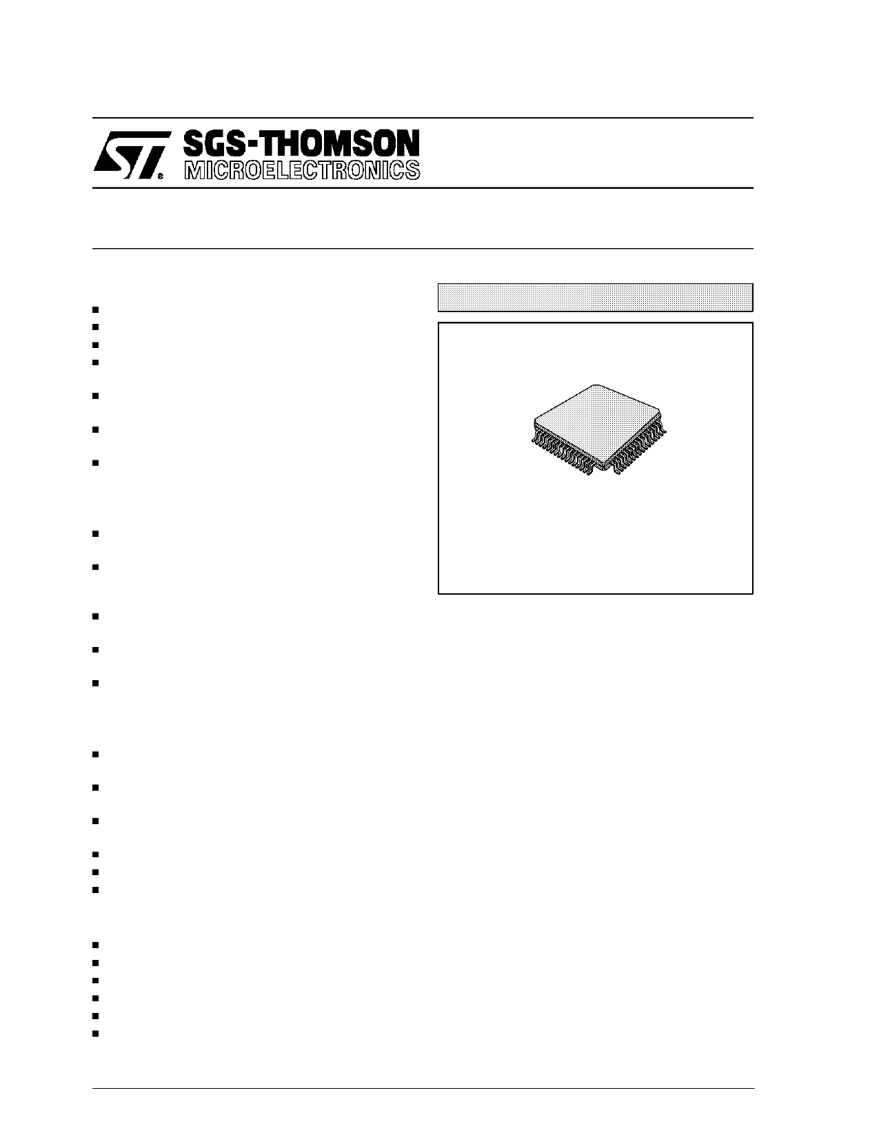
PQFP64
ORDERING NUMBER: L6245
DESCRIPTION
The L6245 contains in a single chip all the func-
tions to operate a sensorless brushless (DC) mo-
tor and a voice coil motor, suitable for hard disk
drive applications.
The device is configured to interface directly to
an 8 bit parallel microprocessor bus, and has a
register based architecture to reduce number of
interconnection lines. All the positioning loop for
sensorless spindle is integrated, including BEMF
sensing, digital masking, digital delay and se-
quencing. All timing function are performed digi-
tally, thus no external filtering components are re-
quired.
The VCM driver is a transconductance amplifier,
able to provide 2 different current ranges, suitable
for seeking or tracking of the head actuator.
When a low voltage is detected, a monitor, in se-
quence, resets the internal registers, puts in tris-
tate the spindle powers, retracts the actuator, and
applies the dynamic brake of the spindle.
The L6245 is realized in Multipower-BCD 2 tech-
nology, which combine isolate DMOS power tran-
sistors with CMOS and Bipolar circuits in the
same monolithic layer, and is assembled in a 64-
pin PQFP.
October 1992
1/15
This is advanced information on a new product now in development or undergoing evaluation. Details are subject to change without notice.
1 page 
L6245
PIN DESCRIPTION (continued)
Pin Number Pin Name Pin Type
44
SYNTH_HALL
O
49, 50,
58
46
56
51
SPIN SENSE
1,2,3
PWM_OFFT
SLEW
S_COMP
A
A
A
A
Description
A TTL compatible signal that emulates one of the Hall signals.
SYNTH_HALL is an open drain output with an internal 20KΩ pull-up.
The current sensing resistors is connected from these pins to ground.
A parallel R-C from this pin to ground sets the PWM mode OFF time.
A resistor from this pin to ground sets the slew rate of the driver.
An R-C network from this pin to GND sets the spin driver
compensation.
VCM Driver and 8 bit D/A
Pin Number
8
9
21
14
23
Pin Name
VCM_DAC
VCM_CMD
VCM_COMP
VCM_RS1
VCM_RS2
Pin Type
O
I
A
A
A
13
VCM+
O
15
VCM-
O
20
OV_VO LT
O
19
OV_CUR
O
16 OV_SUM– I
18
OV_SUM_OUT
O
Description
The output of an 8 bit D/A used to command the VCM driver.
VCM driver input command which is relative to VREF.
An R-C network from this pin to ground compensates the VCM driver.
The high gain current sense resistor is attached from this pin to ground.
The low gain current sense resistor is connected from this pin to
VCM_RS1
One end of the load is attached to this pin (Positive).
The other end of the load is attached to this pin (Negative).
A voltage which is proportional to the voltage across the load,
referenced to VREF.
A voltage which is proportional to the current through the load,
referenced to VREF.
Over-velocity summing op-amp inverting input.
Over-velocity summing op-amp output.
22
ISENSE
O A voltage which is proportional to the current through the VCM load as
sensed by the sense resistor. This signal is enabled by setting bit 2 in
the VCM Control Register.
54 VCM_STRB I The 8 bit input to the VCM D/A is updated on the rising edge of
VCM_STRB.
Solenoid Pre-drivers and Power Down Sequencing
Pin Number
11,55,
63
Pin Name
V_RECIR
Pin Type
P
2
LOAD_SOL
O
1
UNLOAD_SOL
O
4
PD_SEQ_CAP
A
52
BRK_DLY
A
Description
Under normal conditions, power is supplied to various blocks via the
V_RECIR pin. When external power is removed, energy stored in the
rotating spindle is converted to a voltage which supplies the park circuit.
When a logic one is written to bit 3 of the VCM Control Register,
current is sourced from the LOAD_SOL pin. Otherwise, the pin is high
impedance.
When a logic one is written to bit 4 of the VCM Control Register,
current is sourced from the UNLOAD_SOL pin. Otherwise, the pin is
high impedance.
When power is removed, the charge stored on this capacitor keeps
selected blocks alive long enough to effect an orderly power down.
An external parallel RC network from this point to ground delays
activation of the dynamic brake after power is removed.
5/15
5 Page 
REGISTER DEFINITION and 3bit Address Code
Table 1: Status Register (A.C. 001)
Bit Name
7 NC
6 NC
5 NC
4 NC
3 REVERSE SPIN
2 OVER TEMP.
1 SPIN SENSE
0 OVER VEL SET
POR Initial
Value
1
1
0
1
L6245
Table 5: Spin D/A Register (A.C. 101)
Bit Name
7 Most Significant Bit
6
5
4
3
2
1
0 Least Significant Bit
POR Initial
Value
0
0
0
0
0
0
0
0
Table 2: VCM Driver Register (A.C. 010)
Bit Name
7 NC
6 NC
5 NC
4 UNLOAD HD
3 LOAD HD
2 ENABLE ISENSE
1 HIGH GAIN VCM
0 ENABLE VCM
POR Initial
Value
0
0
0
0
0
Table 6: Interrupt Mask Register (A.C. 110)
Bit Name
POR Initial
Value
7 NC
6 NC
5 NC
4 NC
3 NC
2 MASK REV Spin
1 MASK OVER TEMP ERROR
0 MASK OVER VEL ERROR
0
0
0
Table 3: Spin Control Register (A.C. 011)
Bit Name
7 NC
6 LINEAR/PWM
5 INCREMENT STATE
4 RESET STATE
3 RUN/SEARCH
2 UNI/BI
1 HIGH GAIN SPIN
0 ENABLE Spin
POR Initial
Value
0
0
0
0
0
0
0
0
Table 4: VCM D/A Register (A.C. 100)
Bit Name
7 Most Significant Bit
6
5
4
3
2
1
0 Least Significant Bit
POR Initial
Value
0
0
0
0
0
0
0
0
Table 7: Phase Delay Register (A.C. 111)
Bit Name
7 NC
6 NC
5 NC
4 NC
3 Most Significant Bit
2
1
0 Least Significant Bit
POR Initial
Value
0
0
0
0
SYSTEM BUS DESCRIPTION
The system bus is designed as a data acknow-
ledge handshanking bus. At the beginning of the
bus cycle the address and chip select are de-
coded transparently and qualified with read or
write going low. On a read operation, data must
not be driven for 5nsec after read goes low to al-
low the bus to clear. Once data is driven, data ac-
knowledge is driven low to notify the processor
that data is on the bus and ready to be read. The
processor reads the data and responds by raising
read. This is an indication that the processor has
compleated the read and cycle is complete. Data
acknowledge and data must go to high im-
pedence within 20ns to clear the bus for the next
11/15
11 Page | ||
| Páginas | Total 15 Páginas | |
| PDF Descargar | [ Datasheet L6245.PDF ] | |
Hoja de datos destacado
| Número de pieza | Descripción | Fabricantes |
| L6242 | VOICE COIL MOTOR DRIVER | STMicroelectronics |
| L6243 | VOICE COIL MOTOR DRIVER | STMicroelectronics |
| L6243D | VOICE COIL MOTOR DRIVER | STMicroelectronics |
| L6243DS | VOICE COIL MOTOR DRIVER | STMicroelectronics |
| Número de pieza | Descripción | Fabricantes |
| SLA6805M | High Voltage 3 phase Motor Driver IC. |
Sanken |
| SDC1742 | 12- and 14-Bit Hybrid Synchro / Resolver-to-Digital Converters. |
Analog Devices |
|
DataSheet.es es una pagina web que funciona como un repositorio de manuales o hoja de datos de muchos de los productos más populares, |
| DataSheet.es | 2020 | Privacy Policy | Contacto | Buscar |