|
|
|
PDF ICX229AKB Data sheet ( Hoja de datos )
| Número de pieza | ICX229AKB | |
| Descripción | Diagonal 4.5mm (Type 1/4) CCD Image Sensor | |
| Fabricantes | Sony | |
| Logotipo | ||
Hay una vista previa y un enlace de descarga de ICX229AKB (archivo pdf) en la parte inferior de esta página. Total 18 Páginas | ||
|
No Preview Available !
ICX229AKB
Diagonal 4.5mm (Type 1/4) CCD Image Sensor for PAL Color Video Cameras
Description
The ICX229AKB is an interline CCD solid-state
image sensor suitable for PAL color video cameras.
Compared with the current product ICX209AKB,
smear charactristics are improved drastically and
power consumption is reduced. Ye, Cy, Mg, and G
complementary color mosaic filters are used. High
sensitivity and high saturation signal are achieved by
Super HAD CCD technology.
This chip features a field period readout system and
an electronic shutter with variable charge-storage time.
Also, this outline is miniaturized by using original
packege.
Features
• Maximum package dimensions: φ8mm
• Low smear (–100dB Typ.at F5.6)
• Low power consumption (–38% compared with ICX209AKB)
• High sensitivity (+3dB at F1.2 compared with ICX209AKB)
• High saturation signal
• Supply voltage: 12V
• Horizontal register: 3.3V drive
• Reset gate:
3.3V drive
• No voltage adjustment
(Reset gate and substrate bias are not adjusted.)
• High resolution, low dark current
• Excellent antiblooming characteristics
• Continuous variable-speed shutter
• Recommended range of exit pupil distance: –20 to –100mm
• Ye, Cy, Mg, and G complementary color mosaic filters on chip
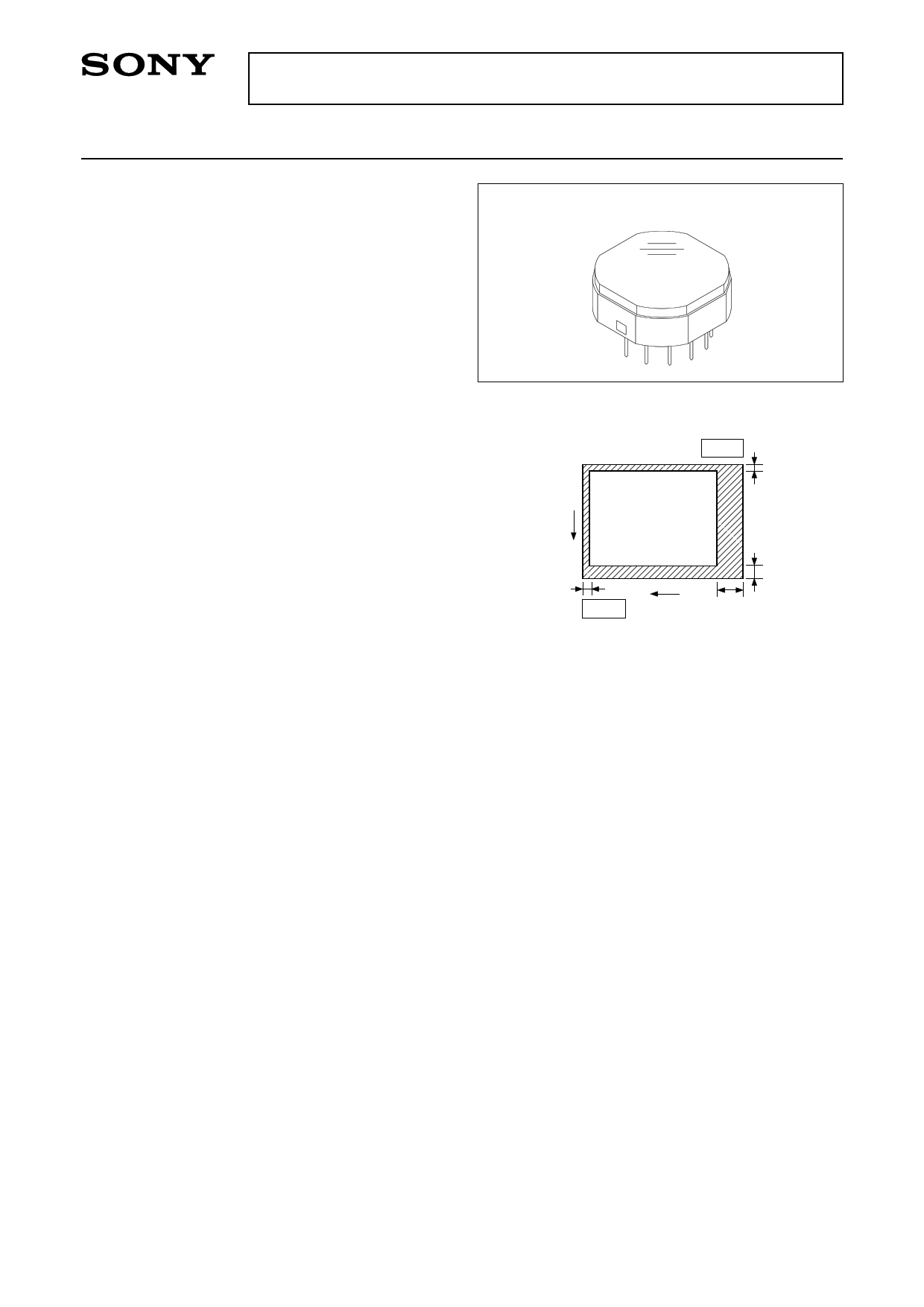
13 pin PCA (Ceramic)
Pin 1
2
V
3
Pin 8
H
12
40
Optical black position
(Top View)
Device Structure
• Interline CCD image sensor
• Image size:
Diagonal 4.5mm (Type 1/4)
• Number of effective pixels: 752 (H) × 582 (V) approx. 440K pixels
• Total number of pixels: 795 (H) × 596 (V) approx. 470K pixels
• Chip size:
4.34mm (H) ×3.69mm (V)
• Unit cell size:
4.85µm (H) × 4.65µm (V)
• Optical black:
Horizontal (H) direction: Front 3 pixels, rear 40 pixels
Vertical (V) direction: Front 12 pixels, rear 2 pixels
• Number of dummy bits: Horizontal 22
Vertical 1 (even fields only)
• Substrate material:
Silicon
Sony reserves the right to change products and specifications without prior notice. This information does not convey any license by
any implication or otherwise under any patents or other right. Application circuits shown, if any, are typical examples illustrating the
operation of the devices. Sony cannot assume responsibility for any problems arising out of the use of these circuits.
–1–
E01935
1 page 
ICX229AKB
Drive Clock Waveform Conditions
(1) Readout clock waveform
100%
90%
10%
0%
VVT
tr twh
(2) Vertical transfer clock waveform
Vφ1
VVH1
VVHH
VVH
VVHH
VVHL
VVHL
φM
φM
2
tf
0V
Vφ3
VVHL
VVHH
VVHH
VVH3
VVHL
VVH
VVL
VVL1
VVLH
VVLL
Vφ2
VVHH
VVH2 VVHL
VVHH
VVH
VVHL
VVL3
VVL
VVLL
VVLH
Vφ4
VVH
VVHH
VVHH
VVHL
VVHL
VVH4
VVL2VVLH
VVLL
VVL
VVH = (VVH1 + VVH2)/2
VVL = (VVL3 + VVL4)/2
VφV = VVHn – VVLn (n = 1 to 4)
VVLH
VVLL
VVL4
–5–
VVL
5 Page 
ICX229AKB
5. Video signal shading
Set to standard imaging condition III. With the lens diaphragm at F5.6 to F8, adjust the luminous intensity
so that the average value of the Y signal output is 200mV. Then measure the maximum (Ymax [mV]) and
minimum (Ymin [mV]) values of the Y signal and substitute the values into the following formula.
SHy = (Ymax – Ymin)/200 × 100 [%]
6. Uniformity between video signal channels
Set to standard imaging condition II. Adjust the luminous intensity so that the average value of the Y signal
output is 200mV, and then measure the maximum (Crmax, Cbmax [mV]) and minimum (Crmin, Cbmin
[mV]) values of the R – Y and B – Y channels of the chroma signal and substitute the values into the
following formula.
∆Sr = | (Crmax – Crmin)/200 | × 100 [%]
∆Sb = | (Cbmax – Cbmin)/200 | × 100 [%]
7. Dark signal
Measure the average value of the Y signal output (Ydt [mV]) with the device ambient temperature 60°C and
the device in the light-obstructed state, using the horizontal idle transfer level as a reference.
8. Dark signal shading
After measuring 7, measure the maximum (Ydmax [mV]) and minimum (Ydmin [mV]) values of the Y signal
output and substitute the values into the following formula.
∆Ydt = Ydmax – Ydmin [mV]
9. Flicker
1) Fy
Set to standard imaging condition II. Adjust the luminous intensity so that the average value of the Y signal
output is 200mV, and then measure the difference in the signal level between fields (∆Yf [mV]). Then
substitute the value into the following formula.
Fy = (∆Yf/200) × 100 [%]
2) Fcr, Fcb
Set to standard imaging condition II. Adjust the luminous intensity so that the average value of the Y signal
output is 200mV, insert an R or B filter, and then measure both the difference in the signal level between
fields of the chroma signal (∆Cr, ∆Cb) as well as the average value of the chroma signal output (CAr, CAb).
Substitute the values into the following formula.
Fci = (∆Ci/CAi) × 100 [%] (i = r, b)
– 11 –
11 Page | ||
| Páginas | Total 18 Páginas | |
| PDF Descargar | [ Datasheet ICX229AKB.PDF ] | |
Hoja de datos destacado
| Número de pieza | Descripción | Fabricantes |
| ICX229AK | CCD Image Sensor with Square Pixel for Color Cameras | Sony |
| ICX229AKB | Diagonal 4.5mm (Type 1/4) CCD Image Sensor | Sony |
| Número de pieza | Descripción | Fabricantes |
| SLA6805M | High Voltage 3 phase Motor Driver IC. |
Sanken |
| SDC1742 | 12- and 14-Bit Hybrid Synchro / Resolver-to-Digital Converters. |
Analog Devices |
|
DataSheet.es es una pagina web que funciona como un repositorio de manuales o hoja de datos de muchos de los productos más populares, |
| DataSheet.es | 2020 | Privacy Policy | Contacto | Buscar |