|
|
|
PDF GTLP6C816A Data sheet ( Hoja de datos )
| Número de pieza | GTLP6C816A | |
| Descripción | LVTTL-to-GTLP Clock Driver | |
| Fabricantes | Fairchild Semiconductor | |
| Logotipo | ||
Hay una vista previa y un enlace de descarga de GTLP6C816A (archivo pdf) en la parte inferior de esta página. Total 7 Páginas | ||
|
No Preview Available !
August 1998
Revised August 1999
GTLP6C816A
LVTTL-to-GTLP Clock Driver
General Description
The GTLP6C816A is a clock driver that provides LVTTL to
GTLP signal level translation (and vice versa). The device
provides a high speed interface between cards operating at
LVTTL logic levels and a backplane operating at GTL(P)
logic levels. High speed backplane operation is a direct
result of GTL(P)’s reduced output swing (<1V), reduced
input threshold levels and output edge rate control. The
edge rate control minimizes bus settling time. GTLP is a
Fairchild Semiconductor derivative of the Gunning Trans-
ceiver logic (GTL) JEDEC standard JESD8-3.
Fairchild’s GTL(P) has internal edge-rate control and is
process, voltage, and temperature (PVT) compensated. Its
function is similar to BTL and GTL but with different output
levels and receiver threshold. GTLP output LOW level is
typically less than 0.5V, the output level HIGH is 1.5V and
the receiver threshold is 1.0V.
Features
s Interface between LVTTL and GTLP logic levels
s Edge Rate Control to minimize noise on the GTLP port
s Power up/down high impedance for live insertion
s 1:6 fanout clock driver for LVTTL port
s 1:2 fanout clock driver for GTLP port
s LVTTL compatible driver and control inputs
s Flow through pinout optimizes PCB layout
s Open drain on GTLP to support wired-or connection
s A Port source/sink −24/+24 mA
s B Port sink 50 mA
s −40°C to +85°C temperature capability
s Low voltage version of GTLP6C816
Ordering Code:
Order Number Package Number Package Description
GTLP6C816AMTC
MTC24
24-Lead Thin Shrink Small Outline Package (TSSOP), JEDEC MO-153, 4.4mm Wide
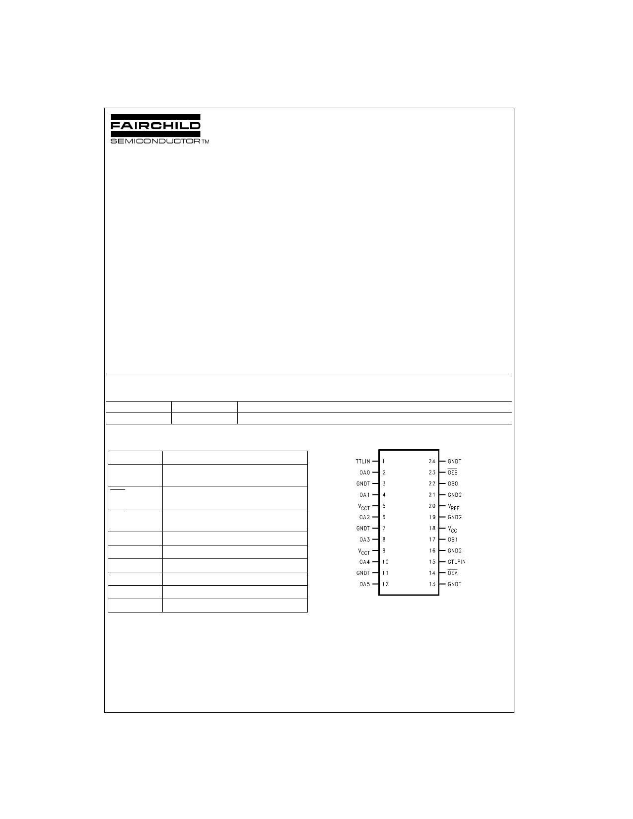
Pin Descriptions
Connection Diagram
Pin Names
Description
TTLIN, GTLPIN Clock Inputs
(LVTTL and GTLP respectively)
OEB
Output Enable (Active LOW)
GTLP Port (LVTTL Levels)
OEA
Output Enable (Active LOW)
TTL Port (LVTTL Levels)
VCCT.GNDT
VCC
GNDG
TTL Output Supplies
Internal Circuitry VCC
OBn GTLP Output Grounds
VREF
OA0–OA5
Voltage Reference Input
TTL Buffered Clock Outputs
OB0–OB1
GTLP Buffered Clock Outputs
© 1999 Fairchild Semiconductor Corporation DS500179
www.fairchildsemi.com
1 page 
AC Electrical Characteristics
Over recommended range of supply voltage and operating free air temperature. VREF = 1.0V (unless otherwise noted).
CL = 30 pF for OBn-Port and CL = 50 pF for OAn-Port.
Symbol
From (Input)
To (Output)
Min
Typ
(Note 6)
Max
fTOGGLE
TTLIN
GTLPIN
OBn
OAn
175
175
tPLH
tPHL
TTLIN
OBn
1.3 2.3 4.0
0.9 2.6 4.3
tPLH
tPHL
tRISE
tFALL
tRISE
tFALL
OEB
OBn
Transition Time, OB Outputs (20% to 80%)
Transition Time, OB outputs (20% to 80%)
Transition Time, OA outputs (10% to 90%)
Transition Time, OA outputs (10% to 90%)
1.5 2.6 4.1
1.2 2.5 4.1
1.3
1.3
1.2
2.0
tPZH, tPZL
OEA
tPLZ, tPHZ
tPLH GTLPIN
tPHL
Note 6: All typical values are at VCC = 3.3 V and TA = 25°C.
OAn
OAn
0.5 2.9 4.8
0.5 2.4 4.4
1.9 3.6 5.7
2.1 3.5 5.3
Units
MHz
ns
ns
ns
ns
ns
ns
Extended Electrical Characteristics
Over recommended ranges of supply voltage and operating free-air temperature VREF = 1.0V (unless otherwise noted).
CL = 30 pF for B Port and CL = 50 pF for A Port
Symbol
From
To
Typ
Min Max
(Input)
(Output)
(Note 7)
Unit
tOSLH (Note 8)
AB
tOSHL (Note 8)
AB
tPS (Note 9)
AB
tPV(HL) (Note 10)(Note 11)
A
B
tOSLH (Note 8)
BA
tOSHL (Note 8)
BA
tOST (Note 8)
BA
tPS (Note 9)
BA
tPV (Note 10)
BA
Note 7: All typical values are at VCC = 3.3 V and TA = 25°C.
0.1 0.2
0.1 0.6
0.3 1.0
1.3
0.1 0.7
0.1 0.4
0.2 1.1
0.1 1.0
2.4
ns
ns
ns
ns
ns
ns
ns
Note 8: tOSHL/tOSLH and tOST – Output-to-Output skew is defined as the absolute value of the difference between the actual propagation delay for all outputs
within the same packaged device. The specifications are given for specific worst case VCC and temperature and apply to any outputs switching in the same
direction dither HIGH-to-LOW (tOSHL) or LOW-to-HIGH (tOSLH) or in opposite directions both HL and LH (tOST). This parameter is guaranteed by design and
statistical process distribution. Actual skew values between the GTLP outputs could vary on the backplane due to the loading and impedance seen by the
device.
Note 9: tPS – Pin or Transition skew is defined as the difference between the LOW-to-HIGH transition and the HIGH-to-LOW transition on the same pin. The
parameter is measured across all the outputs of the same chip is specified for a specific worst case VCC and temperature. This parameter is guaranteed by
design and statistical process distribution. Actual skew values between the GTLP outputs could vary on the backplane due to the loading and impedance
seen by the device.
Note 10: tPV – Part-to-Part skew is defined as the absolute value of the difference between the actual propagation delay for all outputs from device-to-device.
The parameter is specified for a specific worst case VCC and temperature. This parameter is guaranteed by design and statistical process distribution. Actual
skew values between the GTLP output could vary on the backplane due to the loading and impedance seen by the device.
Note 11: Due to the open drain structure on GTLP outputs tOST and tPV(LH) in the A-to-B direction are not specified. Skew on these paths is dependent on the
VTT and RT values on the backplane.
5 www.fairchildsemi.com
5 Page | ||
| Páginas | Total 7 Páginas | |
| PDF Descargar | [ Datasheet GTLP6C816A.PDF ] | |
Hoja de datos destacado
| Número de pieza | Descripción | Fabricantes |
| GTLP6C816 | GTLP-to-TTL 1:6 Clock Driver | Fairchild Semiconductor |
| GTLP6C816A | LVTTL-to-GTLP Clock Driver | Fairchild Semiconductor |
| GTLP6C816AMTC | LVTTL-to-GTLP Clock Driver | Fairchild Semiconductor |
| GTLP6C816MTC | GTLP-to-TTL 1:6 Clock Driver | Fairchild Semiconductor |
| Número de pieza | Descripción | Fabricantes |
| SLA6805M | High Voltage 3 phase Motor Driver IC. |
Sanken |
| SDC1742 | 12- and 14-Bit Hybrid Synchro / Resolver-to-Digital Converters. |
Analog Devices |
|
DataSheet.es es una pagina web que funciona como un repositorio de manuales o hoja de datos de muchos de los productos más populares, |
| DataSheet.es | 2020 | Privacy Policy | Contacto | Buscar |