|
|
|
PDF 24LC174 Data sheet ( Hoja de datos )
| Número de pieza | 24LC174 | |
| Descripción | EEPROM | |
| Fabricantes | Microchip | |
| Logotipo | ||
Hay una vista previa y un enlace de descarga de 24LC174 (archivo pdf) en la parte inferior de esta página. Total 14 Páginas | ||
|
No Preview Available !
Obsolete Device
24LC174
16K 2.5V Cascadable I2C™ Serial EEPROM with OTP Security Page
FEATURES
• Single supply with operation down to 2.5V
• 16 bytes OTP Secure Memory
• Low power CMOS technology
- 1 mA active current typical
- 10 µA standby current typical at 5.5V
- 5 µA standby current typical at 3.0V
• Organized as eight blocks of 256 bytes (8 x 256 x 8)
• 2-wire serial interface bus, I2C compatible
• Functional address inputs for cascading up to 8
devices
• Schmitt trigger, filtered inputs for noise suppression
• Output slope control to eliminate ground bounce
• 100 kHz (2.5V) and 400 kHz (5V) compatibility
• Self-timed write cycle (including auto-erase)
• Page-write buffer for up to 16 bytes
• 2 ms typical write cycle time for page-write
• Hardware write protect for entire memory
• Can be operated as a serial ROM
• Factory programming (QTP) available
• ESD protection > 4,000V
• 1,000,000 Erase/Write cycles guaranteed
• Data retention > 200 years
• 8-pin DIP, 8-lead SOIC packages
• Available temperature ranges:
- Commercial (C):
0°C to +70°C
- Industrial (I):
-40° to +85°
DESCRIPTION
The Microchip Technology Inc. 24LC174 is a cascad-
able 16K bit Electrically Erasable PROM. The device is
organized as eight blocks of 256 x 8-bit memory with a
2-wire serial interface and provides a specially
addressed OTP (one-time programmable) 16 byte
security block. Low voltage design permits operation
down to 2.5 volts with standby and active currents of
only 5 µA and 1 mA respectively. The 24LC174 also
has a page-write capability for up to 16 bytes of data.
The 24LC174 is available in the standard 8-pin DIP and
8-lead surface mount SOIC packages.
The three select pins, A0, A1, and A2, function as chip
select inputs and allow up to eight devices to share a
common bus, for up to 128K bits total system
EEPROM.
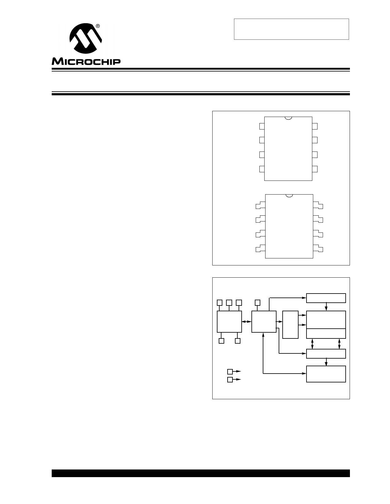
PACKAGE TYPES
PDIP
A0 1
A1 2
A2 3
VSS 4
6 VCC
7 WP
8 SCL
9 SDA
8-lead
SOIC
A0
A1
A2
VSS
1
2
3
4
6 VCC
7 WP
8 SCL
9 SDA
BLOCK DIAGRAM
A0 A1 A2
WP
HV GENERATOR
I/O
CONTROL
LOGIC
MEMORY
CONTROL
LOGIC
XDEC
SDA SCL
EEPROM ARRAY
(8 x 256 x 8)
PAGE LATCHES
YDEC
V CC
V SS
SENSE AMP
R/W CONTROL
I2C is a trademark of Philips Corporation.
2004 Microchip Technology Inc.
DS21101H-page 1
1 page 
3.6 Device Addressing and Operation
A control byte is the first byte received following the
start condition from the master device. The first bit is
always a one. The next three bits of the control byte
are the device select bits (A2, A1, A0). They are used
to select which of the eight devices are to be accessed.
The A1 bit must be the inverse of the A1 device select
pin.
The next three bits of the control byte are the block
select bits (B2, B1, B0). They are used by the master
device to select which of the eight 256 word blocks of
memory are to be accessed. These bits are in effect
the three most significant bits of the word address.
The last bit of the control byte defines the operation to
be performed. When set to one a read operation is
selected, when set to zero a write operation is selected.
Following the start condition, the 24LC174 looks for the
slave address for the device selected. Depending on
the state of the R/W bit, the 24LC174 will select a read
or write operation.
Operation Control Code Block Select R/W
Read
Write
1 A2 A1 A0 Block Address
1 A2 A1 A0 Block Address
1
0
FIGURE 3-2: CONTROL BYTE
ALLOCATION
START
READ/WRITE
SLAVE ADDRESS
R/W A
1 A2 A1 A0 B2 B1 B0
MSB
LSB
24LC174
4.0 WRITE OPERATION
4.1 Byte Write
Following the start condition from the master, the
device code (4 bits), the block address (3 bits), and the
R/W bit which is a logic low is placed onto the bus by
the master transmitter. This indicates to the addressed
slave receiver that a byte with a word address will fol-
low after it has generated an acknowledge bit during
the ninth clock cycle. Therefore the next byte transmit-
ted by the master is the word address and will be writ-
ten into the address pointer of the 24LC174. After
receiving another acknowledge signal from the
24LC174 the master device will transmit the data word
to be written into the addressed memory location. The
24LC174 acknowledges again and the master gener-
ates a stop condition. This initiates the internal write
cycle, and during this time the 24LC174 will not gener-
ate acknowledge signals (Figure 4-1).
4.2 Page Write
The write control byte, word address and the first data
byte are transmitted to the 24LC174 in the same way
as in a byte write. But instead of generating a stop con-
dition the master transmits up to 16 data bytes to the
24LC174 which are temporarily stored in the on-chip
page buffer and will be written into the memory after the
master has transmitted a stop condition. After the
receipt of each word, the four lower order address
pointer bits are internally incremented by one. The
higher order seven bits of the word address remains
constant. If the master should transmit more than 16
words prior to generating the stop condition, the
address counter will roll over and the previously
received data will be overwritten. As with the byte write
operation, once the stop condition is received an inter-
nal write cycle will begin (Figure 7.3).
Note:
Page write operations are limited to writing
bytes within a single physical page,
regardless of the number of bytes actually
being written. Physical page boundaries
start at addresses that are integer multiples
of the page buffer size (or ‘page size’) and
end at addresses that are integer multiples
of [page size - 1]. If a page write command
attempts to write across a physical page
boundary, the result is that the data wraps
around to the beginning of the current page
(overwriting data previously stored there),
instead of being written to the next page as
might be expected. It is therefore neces-
sary for the application software to prevent
page write operations that would attempt to
cross a page boundary.
2004 Microchip Technology Inc.
DS21101H-page 5
5 Page 
24LC174
24LC174 Product Identification System
To order or to obtain information, e.g., on pricing or delivery, please use the listed part numbers, and refer to the factory or the listed
sales offices.
24LC174 –
/P
Package:
P = Plastic DIP (300 mil Body), 8-lead
SN = Plastic SOIC (150 mil Body), 8-lead
Temperature
Range:
Blank = 0°C to +70°C
I = -40°C to +85°C
Device:
24LC174 16K I2C Serial EEPROM
24LC174T 16K I2C Serial EEPROM (Tape and Reel)
Sales and Support
Data Sheets
Products supported by a preliminary Data Sheet may have an errata sheet describing minor operational differences and recom-
mended workarounds. To determine if an errata sheet exists for a particular device, please contact one of the following:
1. Your local Microchip sales office
2. The Microchip Corporate Literature Center U.S. FAX: (602) 786-7277
3. The Microchip Worldwide Site (www.microchip.com)
Please specify which device, revision of silicon and Data Sheet (include Literature #) you are using.
New Customer Notification System
Register on our web site (www.microchip.com/cn) to receive the most current information on our products.
2004 Microchip Technology Inc.
DS21101H-page 11
11 Page | ||
| Páginas | Total 14 Páginas | |
| PDF Descargar | [ Datasheet 24LC174.PDF ] | |
Hoja de datos destacado
| Número de pieza | Descripción | Fabricantes |
| 24LC174 | EEPROM | Microchip |
| Número de pieza | Descripción | Fabricantes |
| SLA6805M | High Voltage 3 phase Motor Driver IC. |
Sanken |
| SDC1742 | 12- and 14-Bit Hybrid Synchro / Resolver-to-Digital Converters. |
Analog Devices |
|
DataSheet.es es una pagina web que funciona como un repositorio de manuales o hoja de datos de muchos de los productos más populares, |
| DataSheet.es | 2020 | Privacy Policy | Contacto | Buscar |