|
|
|
PDF SLG8SP513 Data sheet ( Hoja de datos )
| Número de pieza | SLG8SP513 | |
| Descripción | Clock Synthesizer | |
| Fabricantes | Silego Technology | |
| Logotipo | ||
Hay una vista previa y un enlace de descarga de SLG8SP513 (archivo pdf) en la parte inferior de esta página. Total 24 Páginas | ||
|
No Preview Available !
SLG8SP513
Clock Synthesizer for Intel
Mobile PCI-Express Chipset
Features
• Low Power CK505 compatible clock synthesizer
• SLG8SP513 is a cost reduced CK505 with integrated volt-
age regulator for mobile applications
• Scalable Low Voltage VDD I/O (3.3V to 1.05V) to reduce
power consumption
• Low Power differential outputs with integrated series ter-
mination resistors (50 ohm resistor to GND and 33 ohm
series resistor not needed)
• Integrated CK_SSCD function to provide additional
Spread Spectrum support for GMCH
• CLK_REQ# inputs to support SRC clock power manage-
ment
• 64 pin QFN Package
Output Summary
• 2- differential CPU clock outputs @ 0.7V
• 1 - selectable differential CPU/SRC clock output @ 0.7V
• 1 - selectable differential DOT96/SRC clock output @ 0.7V
• 8 - differential Serial Reference Clock (SRC) clock outputs
@ 0.7V
• 1 - selectable LCDCLK/27M clock output
• 1 - single-ended 48MHz clock output @ 3.3V
• 6 - single-ended 33MHz clock outputs @ 3.3V
• 1 - single-ended 14.318MHz clock output @ 3.3V
Table 1. Frequency Select Table (FS_C, FS_B, FS_A)
FFF
SSS
___
CBA
000
001
010
011
100
101
110
111
CPU
(MHz)
266.6
133.3
200.0
166.6
333.3
100.0
400.0
SRC
(MHz)
100.0
100.0
100.0
100.0
100.0
100.0
100.0
PCI REF
(MHz) (MHz)
33.3 14.318
33.3 14.318
33.3 14.318
33.3 14.318
33.3 14.318
33.3 14.318
33.3 14.318
Reserved
DOT_
96
(MHz)
96.0
96.0
96.0
96.0
96.0
96.0
96.0
USB
(MHz)
48.0
48.0
48.0
48.0
48.0
48.0
48.0
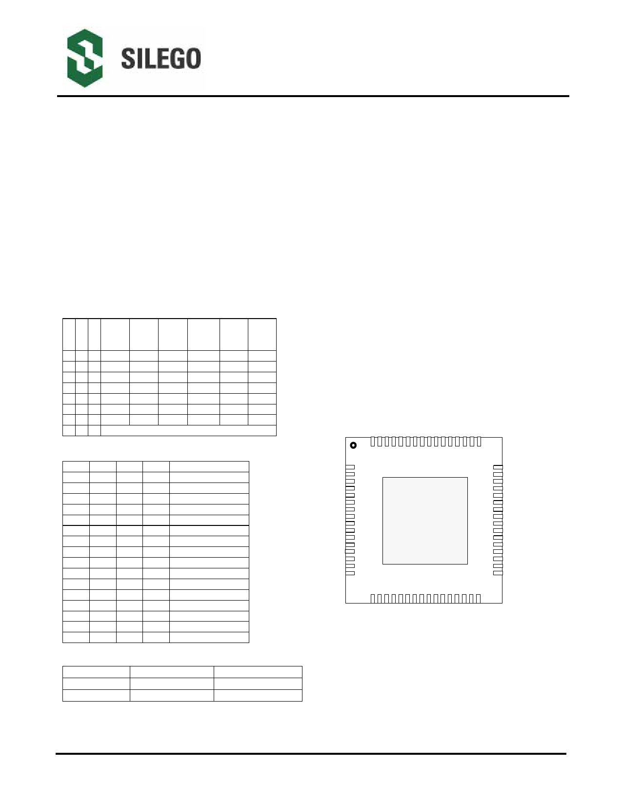
Pin Configuration
(Top View)
Table 2. LCDCLK & 27M_SS Spread Spectrum Table
B1b5
0
0
0
0
0
0
0
0
1
1
1
1
1
1
1
1
B1b3
0
0
0
0
1
1
1
1
0
0
0
0
1
1
1
1
B1b2
0
0
1
1
0
0
1
1
0
0
1
1
0
0
1
1
B1b1
0
1
0
1
0
1
0
1
0
1
0
1
0
1
0
1
Spread Spectrum %
Reserved
Reserved
-0.50% SS
-1.00% SS
-1.50% SS
-2.00% SS
-2.50% SS
Reserved
Reserved
Reserved
+/-0.25% SS
+/-0.50% SS
+/-0.75% SS
+/-1.00% SS
+/-1.25% SS
Reserved
VSS_REF
XTAL_OUT
XTAL_IN
VDD_REF
REF/FS_C/TEST_SEL
SDA
SCL
PCI_0/CLKREQ_A#
VDD_PCI
PCI_1/CLKREQ_B#
PCI_2
PCI_3
^PCI_4/SEL_LCDCLK#
PCIF_5/ITP_EN
VSS_PCI
VDD_48
1
2
3
4
5
6
7
8
9
10
11
12
13
14
15
16
SLG8SP513
48 SRC_6
47 SRC_6#
46 VDD_SRC
45 PCI_STOP#
44 CPU_STOP#
43 VDD_SRC_I/O
42 SRC_10#
41 SRC_10
40 SRC_11/CLKREQ_H#
39 SRC_11#/CLKREQ_G#
38 SRC_9#
37 SRC_9
36 VSS_SRC
35 SRC_4#
34 SRC_4
33 VDD_SRC_I/O
Table 3. SEL_LCDCLK# Input Functional Table
SEL_LCDCLK#
0
1
Pin 20/21
DOT_96 / DOT_96#
SRC_0 / SRC_0#
Pin 24/25
LCDCLK / LCDCLK#
27M / 27M_SS
^ This pin has internal pull-down to GND
64-Pin QFN
9.0 x 9.0mm body, 0.50mm pitch
Other brands and names may be claimed as the property of others
Silego Technology, Inc.
000-0084513-10
Rev 1.0
Revised July 24, 2007
1 page 
Block Diagram
XTAL_IN
XTAL_OUT
XTAL
SCL, SDA
PD
CPU_STOP#
PCI_STOP#
CKPWRGD
FS_A:C
ITP_EN
TEST_MODE,
TEST_SEL
CLKREQ_A:H#
Serial Interface
&
Control Logic
PLL1
PLL3
PLL4
PLL2
Figure 1. Simplified Block Diagram
SLG8SP513
REF
CPU_0,
CPU_1_AMT
CPU_ITP,
SRC_8
SRC_1:4,
SRC_6:7,
SRC_9:11
PCI_0:4,
PCIF_5
27M
LCDCLK/27M_SS
DOT_96/SRC_0
USB
000-0084513-10
Page 5 of 24
5 Page 
Control Register 2 (continued)
Bit Type
6 RW 48MHz Output Enabled
0 = Disabled
1 = Enabled
5 RW PCIF_5 Output Enabled
0 = Disabled
1 = Enabled
4 RW PCI_4 Output Enabled
0 = Disabled
1 = Enabled
3 RW PCI_3 Output Enabled
0 = Disabled
1 = Enabled
2 RW PCI_2 Output Enabled
0 = Disabled
1 = Enabled
1 RW PCI_1 Output Enabled
0 = Disabled
1 = Enabled
0 RW PCI_0 Output Enabled
0 = Disabled
1 = Enabled
Description/Function
Control Register 3
Bit Type
Description/Function
7 RW SRC_11 Output Enabled
0 = Disabled
1 = Enabled
6 RW SRC_10 Output Enabled
0 = Disabled
1 = Enabled
5 RW SRC_9 Output Enabled
0 = Disabled
1 = Enabled
4 RW SRC_8/CPU_ITP Output Enabled
0 = Disabled
1 = Enabled
3 RW SRC_7 Output Enabled
0 = Disabled
1 = Enabled
2 RW SRC_6 Output Enabled
0 = Disabled
1 = Enabled
1 RW Reserved
0 RW SRC_4 Output Enabled
0 = Disabled
1 = Enabled
000-0084513-10
SLG8SP513
Power up
condition
1
1
1
1
1
1
1
Power up
condition
1
1
1
1
1
1
1
1
Page 11 of 24
11 Page | ||
| Páginas | Total 24 Páginas | |
| PDF Descargar | [ Datasheet SLG8SP513.PDF ] | |
Hoja de datos destacado
| Número de pieza | Descripción | Fabricantes |
| SLG8SP513 | Clock Synthesizer | Silego Technology |
| Número de pieza | Descripción | Fabricantes |
| SLA6805M | High Voltage 3 phase Motor Driver IC. |
Sanken |
| SDC1742 | 12- and 14-Bit Hybrid Synchro / Resolver-to-Digital Converters. |
Analog Devices |
|
DataSheet.es es una pagina web que funciona como un repositorio de manuales o hoja de datos de muchos de los productos más populares, |
| DataSheet.es | 2020 | Privacy Policy | Contacto | Buscar |