|
|
PDF BD9306AFVM Data sheet ( Hoja de datos )
| Número de pieza | BD9306AFVM | |
| Descripción | High-efficiency Switching Regulator | |
| Fabricantes | ROHM Semiconductor | |
| Logotipo | ||
Hay una vista previa y un enlace de descarga de BD9306AFVM (archivo pdf) en la parte inferior de esta página. Total 17 Páginas | ||
|
No Preview Available !
Large Current External FET Controller Type Switching Regulators
Single-output Step-up,High-efficiency
Switching Regulator(Controller Type)
BD9306AFVM
Single-output Step-up,High-efficiency
Switching Regulator(Controller Type)
BD9305AFVM
No.09028EAT04
Description
BD9305AFVM / BD9306AFVM are 1-channel DC/DC converter controllers. Step-down DC/DC converter can be configured
by BD9305AFVM, and Step-up DC/DC converter can be configured by BD9306AFVM. In addition, the master slave function,
which is that the synchronization is possible at the time of multi-connection, is mounted.
Features
1) 1ch PWM Control DC/DC Converter Controller
2) Input Voltage Range:4.2 to 18V
3) Feed Back Voltage:1.25±1.6%
4) Oscillating Frequency Variable:100 to 800kHz
5) Built-in Soft Start Function
6) Standby Current of 0 A (Typ.)
7) Built-in Master / Slave Function
8) Protection Circuit : Under Voltage Lockout Protection Circuit
Thermal Shutdown Circuit
Short Protection Circuit of Timer Latch type
9) MSOP8 Package
Applications
・TV, Power Supply for the TFT-LCD Panels used for LCD TVs, Back Lights
・DSC, DVC, Printer, DVD ,DVD Recorder, Generally Consumer Equipments etc.
Absolute maximum ratings (Ta = 25°C)
Parameter
Symbol
Limit
Unit
Power supply voltage**
Vcc
20
Power dissipation
Pd
588*
Operating temperature range
Topr
-40 to +85
Storage temperature range
Tstg
-55 to +150
Maximum junction temperature
Tjmax
150
* Reduced by 4.7 mW/°C over 25°C, when mounted on a glass epoxy 4-layer board (70 mm 70 mm 1.6 mm)
** Must not exceed Pd.
V
mW
℃
℃
℃
Recommended Operating Ranges (Ta=-40℃ to +85℃)
Parameter
Symbol
Power supply voltage
Control Voltage
Timing Capacity
Timing Resistance
Oscillating frequency
Vcc
VENB
CT
RT
Fosc
Min
4.2
-
100
5
100
Limit
Typ
12
-
-
-
-
Max
18
Vcc
1000
50
800
Unit
V
V
pF
kΩ
kHz
www.rohm.com
© 2009 ROHM Co., Ltd. All rights reserved.
1/14
2009.05 - Rev.A
1 page 
BD9306AFVM, BD9305AFVM
Block Diagram
Technical Note
FB
8
1.25V
Err
COMP
7
GND
6
Vcc
5
Soft
Start
Timer
Latch
Shut Down
Vref
UVLO
TSD
Shut Down
OSC
PWM
DRV
VCC
1
RT
FB
8
1.25V
Err
ENABLE
2
CT
COMP
7
3
ENB
GND
6
4
GD
Vcc
5
Soft
Start
Timer
Latch
Shut Down
Vref
UVLO
TSD
Shut Down
OSC
PWM
DRV
ENABLE
12
RT CT
3
ENB
4
GD
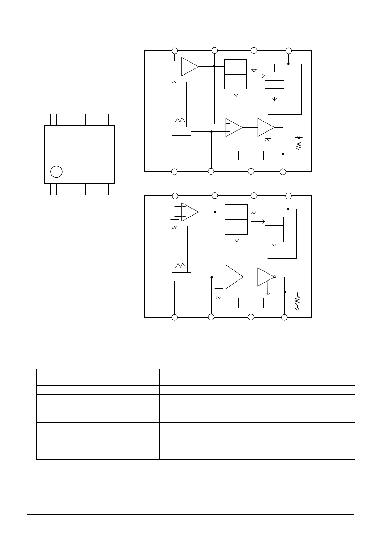
Fig19. Pin Assignment Diagram & Block Diagram (Above:BD9305AFVM / Below:BD9306AFVM)
Pin Assignment and Pin Function
Pin No
Pin Name
1 RT
2 CT
3 ENB
4 GD
5 Vcc
6 GND
7 COMP
8 FB
Function
Timing Resistance connection Pin
Timing Capacity connection Pin
Control Pin
Gate Drive Output Pin
Power Supply Pin
Ground pin
Error amp output Pin
Error amp inversion input Pin
www.rohm.com
© 2009 ROHM Co., Ltd. All rights reserved.
5/14
2009.05 - Rev.A
5 Page 
BD9306AFVM, BD9305AFVM
Technical Note
Example of application
※We recommend the application circuit examples with confidence, but hope that you will thoroughly check the characteristics
over again when putting them to use.
When you change the external circuit constant and use, please make a decision to leave a sufficient margin after taking
into consideration the deviation etc. of external components and ROHM IC, in terms of not only the static characteristic but
also the transient characteristic.
Moreover, please understand that our company can not confirm fully with regard to the patent right.
<Master Slave Function>
The master slave function, which is that the synchronous switching is possible by using these IC of BD9305AFVM /
BD9306AFVM through their multi-connection, is mounted. The following drawing shows an example of connection circuit
in which BD9305AFVM is connected on the master side and BD9306AFVM is connected on the slave side.
VCC
CTL1
BD9305AFVM
(Master Side)
RT
CT
CTL2
CTL0
BD9306AFVM
(Slave Side)
Vo1
Vo2
Fig.31 Master Slave Application Circuit
In the above-mentioned circuit, BD9306AFVM, which is synchronized with the switching frequency determined by RT and
CT of BD9305AFVM that is the master, operates.In addition, the ON/OFF of output can be controlled by connecting the
switch to the COMP terminal. (Refer to the following table)
Output state
Control signal correspondence table
Control signal
Vo1 Vo2
OFF
OFF
OFF
ON
ON OFF
ON ON
*The same in either case of High / Low.
CTL0
Low
High
High
High
CTL1
*
High
Low
Low
CTL2
*
Low
High
Low
Similarly in the case of connecting three or more than three, synchronization is possible by connecting the CT terminal of
Master and the CT terminal of Slave
www.rohm.com
© 2009 ROHM Co., Ltd. All rights reserved.
11/14
2009.05 - Rev.A
11 Page | ||
| Páginas | Total 17 Páginas | |
| PDF Descargar | [ Datasheet BD9306AFVM.PDF ] | |
Hoja de datos destacado
| Número de pieza | Descripción | Fabricantes |
| BD9306AFVM | High-efficiency Switching Regulator | ROHM Semiconductor |
| Número de pieza | Descripción | Fabricantes |
| SLA6805M | High Voltage 3 phase Motor Driver IC. |
Sanken |
| SDC1742 | 12- and 14-Bit Hybrid Synchro / Resolver-to-Digital Converters. |
Analog Devices |
|
DataSheet.es es una pagina web que funciona como un repositorio de manuales o hoja de datos de muchos de los productos más populares, |
| DataSheet.es | 2020 | Privacy Policy | Contacto | Buscar |
