|
|
|
PDF IDT5P90005 Data sheet ( Hoja de datos )
| Número de pieza | IDT5P90005 | |
| Descripción | SERIAL REAL-TIME CLOCK | |
| Fabricantes | Integrated Device Technology | |
| Logotipo | ||
Hay una vista previa y un enlace de descarga de IDT5P90005 (archivo pdf) en la parte inferior de esta página. Total 16 Páginas | ||
|
No Preview Available !
SERIAL REAL-TIME CLOCK
PRELIMINARY DATASHEET
IDT5P90005
Description
The IDT5P90005 is a serial real-time clock (RTC) device
that consumes ultra-low power and provides a full
binary-coded decimal (BCD) clock/calendar. The
clock/calendar provides seconds, minutes, hours, day,
date, month, and year information. The clock operates in
either the 24-hour or 12-hour format with AM/PM indicator.
The end of the month date is automatically adjusted for
months with fewer than 31 days, including corrections for
leap year. Access to the clock/calendar registers is
provided by an I2C interface capable of operating in fast I2C
mode. Built-in Power-sense circuitry detects power failures
and automatically switches to the backup supply,
maintaining time and date operation.
Features
• Packaged in 8-pin SOIC
• Counters for seconds, minutes, hours, days, date,
months, years, and century
• 32 kHz crystal oscillator integrating load capacitance
(12.5 pF) providing exceptional oscillator stability and
high crystal series resistance operation
• Serial interface supports I2C bus (100 or 400 kHz
protocol)
• Ultra low battery supply current of 0.8 µA (typ at 3 V)
• 2.0 to 5.5 V clock operating voltage
• Automatic switch over and deselect circuitry
• Automatic leap year compensation
• Operating temperature of -40 to +85°C
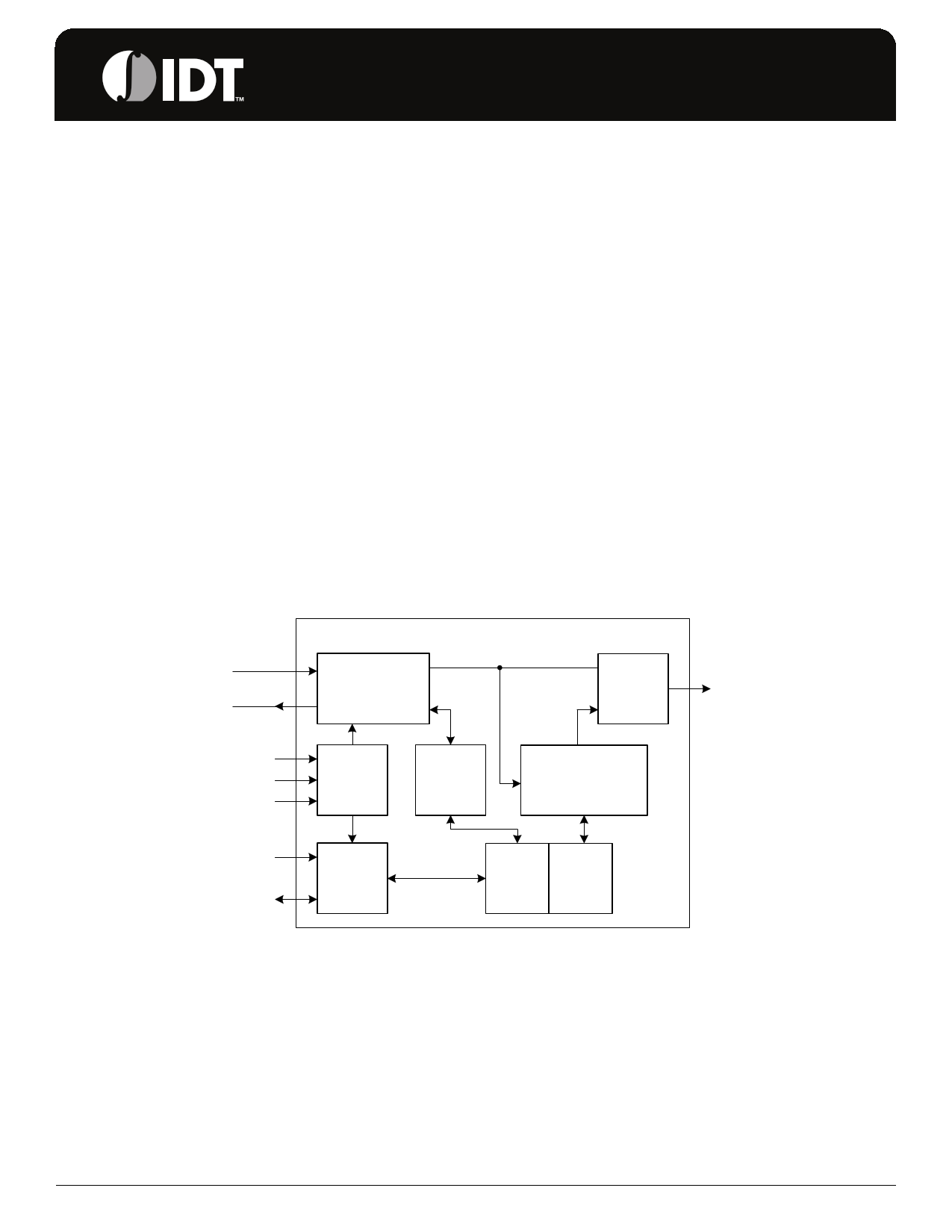
Block Diagram
OSCI
OSCO
VCC
GND
VBAT
SCL
SDA
32.768 kHz
Oscillator and
Divider
1 Hz
MUX/
Buffer
Power
Control
Control
Logic
Clock, Calendar
Counter
I2C
Interface
1 Byte 7 Bytes
Control Buffer
FT/OUT
IDT™ SERIAL REAL-TIME CLOCK
1
IDT5P90005 REV E 031209
1 page 
IDT5P90005
SERIAL REAL-TIME CLOCK
Data Transfer on I2C Serial Bus
RTC
Depending upon the state of the R/W bit, two types of data
transfer are possible:
1) Data transfer from a master transmitter to a slave
receiver. The first byte transmitted by the master is the
slave address. Next follows a number of data bytes. The
slave returns an acknowledge bit after each received byte.
Data is transferred with the most significant bit (MSB) first.
2) Data transfer from a slave transmitter to a master
receiver. The first byte (the slave address) is transmitted by
the master. The slave then returns an acknowledge bit. This
is followed by the slave transmitting a number of data bytes.
The master returns an acknowledge bit after all received
bytes other than the last byte. At the end of the last received
byte, a “not acknowledge” is returned. The master device
generates all of the serial clock pulses and the START and
STOP conditions. A transfer is ended with a STOP condition
or with a repeated START condition. Since a repeated
START condition is also the beginning of the next serial
transfer, the bus is not released. Data is transferred with the
most significant bit (MSB) first.
The IDT5P90005 can operate in the following two modes:
1) Slave Receiver Mode (Write Mode): Serial data and
clock are received through SDA and SCL. After each byte is
received an acknowledge bit is transmitted. START and
STOP conditions are recognized as the beginning and end
of a serial transfer. Address recognition is performed by
hardware after reception of the slave address and direction
bit (see the “Data Write–Slave Receiver Mode” figure). The
slave address byte is the first byte received after the START
condition is generated by the master. The slave address
byte contains the 7-bit IDT5P90005 address, which is
1101000, followed by the direction bit (R/W), which is 0 for
a write. After receiving and decoding the slave address byte
the slave outputs an acknowledge on the SDA line. After the
IDT5P90005 acknowledges the slave address + write bit,
the master transmits a register address to the IDT5P90005.
This sets the register pointer on the IDT5P90005, with the
IDT5P90005 acknowledging the transfer. The master may
then transmit zero or more bytes of data, with the
IDT5P90005 acknowledging each byte received. The
address pointer increments after each data byte is
transferred. The master generates a STOP condition to
terminate the data write.
2) Slave Transmitter Mode (Read Mode): The first byte is
received and handled as in the slave receiver mode.
However, in this mode, the direction bit indicates that the
transfer direction is reversed. Serial data is transmitted on
SDA by the IDT5P90005 while the serial clock is input on
SCL. START and STOP conditions are recognized as the
beginning and end of a serial transfer (see the “Data
Read–Slave Transmitter Mode” figure). The slave address
byte is the first byte received after the START condition is
generated by the master. The slave address byte contains
the 7-bit IDT5P90005 address, which is 1101000, followed
by the direction bit (R/W), which is 1 for a read. After
receiving and decoding the slave address byte the slave
outputs an acknowledge on the SDA line. The IDT5P90005
IDT™ SERIAL REAL-TIME CLOCK
5
IDT5P90005 REV E 031209
5 Page 
IDT5P90005
SERIAL REAL-TIME CLOCK
RTC
AC Electrical Characteristics
Unless stated otherwise, VCC = 2.0 to 5.5 V, Ambient Temperature -40 to +85C
Parameter
Symbol
STANDARD
MODE
Min. Max.
SCL Clock Frequency
Clock Low Period
Clock High Period
SDA and SCL Rise time
SDA and SCL Fall Time
START Condition Hold Time (after this
period the first clock pulse is generated)
fSCL
tLOW
tHIGH
tR
tF
tHD:STA
4.7
4.0
4
100
1
300
START Condition Setup Time (only relevant
for a repeated start condition)
Data Hold Time
Data Setup Time
STOP Condition Setup Time
Time the bus must be free before a new
transmission can start
tSU:STA
tHD:DAT1
tSU:DAT
tSU:STO
tBUF
4.7
0
250
4.0
4.7
FAST MODE
Min.
1.3
0.6
Max.
400
0.3
300
0.6
1.3
100
0.6
1.3
Units
kHz
µs
µs
µs
ns
µs
µs
ns
ns
µs
µs
Note 1: Transmitter must internally provide a hold time to bridge the undefined region (300 ns max) of the falling
edge of SCL.
Power Down/Up Mode AC Waveforms
RTC Power Down/Up AC Characteristics
Parameter1,2
SCL and SDA at VIH before Power Down
SCL and SDA at VIH after Power Up
Symbol
tPD
trec
Min.
0
10
Typ.
Max.
2000
Units
ns
µs
Note 1: Valid for ambient operating temperature: TA = –40 to 85 °C; VCC = 2.0 to 5.5 V (except where noted).
Note 2: VCC fall time should not exceed 5 mV/µs.
IDT™ SERIAL REAL-TIME CLOCK
11
IDT5P90005 REV E 031209
11 Page | ||
| Páginas | Total 16 Páginas | |
| PDF Descargar | [ Datasheet IDT5P90005.PDF ] | |
Hoja de datos destacado
| Número de pieza | Descripción | Fabricantes |
| IDT5P90005 | SERIAL REAL-TIME CLOCK | Integrated Device Technology |
| Número de pieza | Descripción | Fabricantes |
| SLA6805M | High Voltage 3 phase Motor Driver IC. |
Sanken |
| SDC1742 | 12- and 14-Bit Hybrid Synchro / Resolver-to-Digital Converters. |
Analog Devices |
|
DataSheet.es es una pagina web que funciona como un repositorio de manuales o hoja de datos de muchos de los productos más populares, |
| DataSheet.es | 2020 | Privacy Policy | Contacto | Buscar |