|
|
|
PDF FDD7N60NZ Data sheet ( Hoja de datos )
| Número de pieza | FDD7N60NZ | |
| Descripción | N-Channel UniFETTM II MOSFET | |
| Fabricantes | Fairchild Semiconductor | |
| Logotipo | ||
Hay una vista previa y un enlace de descarga de FDD7N60NZ (archivo pdf) en la parte inferior de esta página. Total 9 Páginas | ||
|
No Preview Available !
FDD7N60NZ / FDU7N60NZTU
N-Channel UniFETTM II MOSFET
600 V, 5.5 A, 1.25 Ω
November 2013
Features
• RDS(on) = 1.05 Ω (Typ.) @ VGS = 10 V, ID = 2.75 A
• Low Gate Charge (Typ. 13 nC)
• Low Crss (Typ. 7 pF)
• 100% Avalanche Tested
• Improved dv/dt Capability
• ESD Improved Capability
• RoHS Compliant
Applications
Description
UniFETTM II MOSFET is Fairchild Semiconductor’s high voltage
MOSFET family based on advanced planar stripe and DMOS
technology. This advanced MOSFET family has the smallest on-
state resistance among the planar MOSFET, and also provides
superior switching performance and higher avalanche energy
strength. In addition, internal gate-source ESD diode allows
UniFETTM II MOSFET to withstand over 2kV HBM surge stress.
This device family is suitable for switching power converter appli-
cations such as power factor correction (PFC), flat panel display
(FPD) TV power, ATX and electronic lamp ballasts.
• Lighting
• Uninterruptible Power Supply
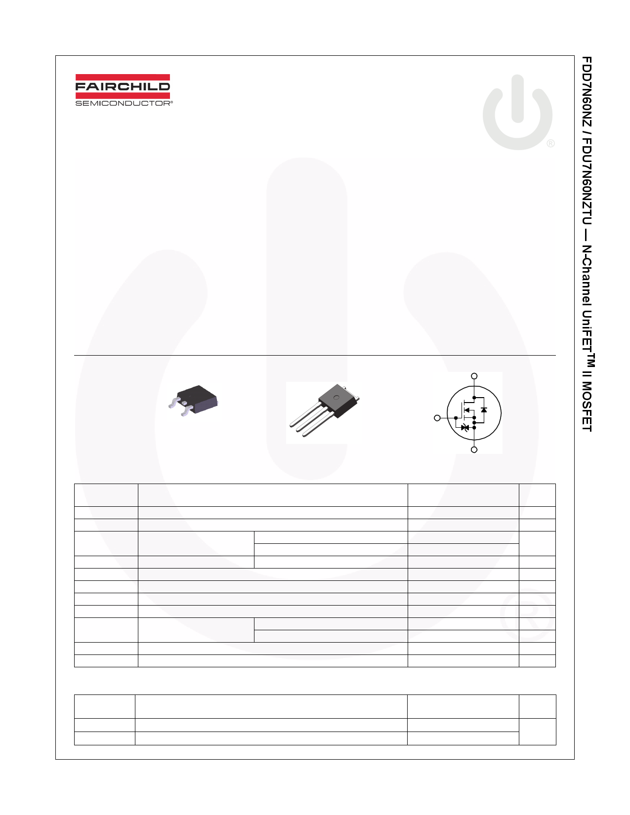
G
S
D
D-PAK
GDS
I-PAK
MOSFET Maximum Ratings TC = 25oC unless otherwise noted.
Symbol
VDSS
VGSS
ID
IDM
EAS
IAR
EAR
dv/dt
PD
TJ, TSTG
TL
Parameter
Drain to Source Voltage
Gate to Source Voltage
Drain Current
Drain Current
- Continuous (TC = 25oC)
- Continuous (TC = 100oC)
- Pulsed
(Note 1)
Single Pulsed Avalanche Energy
(Note 2)
Avalanche Current
(Note 1)
Repetitive Avalanche Energy
(Note 1)
Peak Diode Recovery dv/dt
Power Dissipation
(TC = 25oC)
- Derate Above 25oC
(Note 3)
Operating and Storage Temperature Range
Maximum Lead Temperature for Soldering, 1/8” from Case for 5 Seconds
Thermal Characteristics
Symbol
RθJC
RθJA
Parameter
Thermal Resistance, Junction to Case, Max.
Thermal Resistance, Junction to Ambient, Max.
©2011 Fairchild Semiconductor Corporation
FDD7N60NZ / FDU7N60NZTU Rev. C1
1
D
G
S
FDD7N60NZTM/
FDU7N60NZTU
600
±25
5.5
3.3
22
347
5.5
12.5
10
90
0.7
-55 to +150
300
Unit
V
V
A
A
mJ
A
mJ
V/ns
W
W/oC
oC
oC
FDD7N60NZTM/
FDU7N60NZTU
1.4
90
Unit
oC/W
www.fairchildsemi.com
1 page 
IG = const.
Figure 12. Gate Charge Test Circuit & Waveform
V10GVS
VDS
VGS
RG
RL
VDD
VDS
90%
DUT
VGS 10%
td(on)
tr
t on
Figure 13. Resistive Switching Test Circuit & Waveforms
td(off)
tf
t off
VGS
Figure 14. Unclamped Inductive Switching Test Circuit & Waveforms
©2011 Fairchild Semiconductor Corporation
FDD7N60NZ / FDU7N60NZTU Rev. C1
5
www.fairchildsemi.com
5 Page | ||
| Páginas | Total 9 Páginas | |
| PDF Descargar | [ Datasheet FDD7N60NZ.PDF ] | |
Hoja de datos destacado
| Número de pieza | Descripción | Fabricantes |
| FDD7N60NZ | N-Channel UniFETTM II MOSFET | Fairchild Semiconductor |
| Número de pieza | Descripción | Fabricantes |
| SLA6805M | High Voltage 3 phase Motor Driver IC. |
Sanken |
| SDC1742 | 12- and 14-Bit Hybrid Synchro / Resolver-to-Digital Converters. |
Analog Devices |
|
DataSheet.es es una pagina web que funciona como un repositorio de manuales o hoja de datos de muchos de los productos más populares, |
| DataSheet.es | 2020 | Privacy Policy | Contacto | Buscar |