|
|
|
PDF BD9488F Data sheet ( Hoja de datos )
| Número de pieza | BD9488F | |
| Descripción | Boost 1channel white LED driver | |
| Fabricantes | ROHM Semiconductor | |
| Logotipo | ||
Hay una vista previa y un enlace de descarga de BD9488F (archivo pdf) en la parte inferior de esta página. Total 30 Páginas | ||
|
No Preview Available !
Datasheet
Boost 1channel white LED driver
For large LCDs
BD9488F
●General Description
BD9488F is a high efficiency driver for white LEDs and
designed for large LCDs. This IC is built-in a boost
DCDC converters that employ an array of LEDs as the
light source. BD9488F has some protect function against
fault conditions, such as the over-voltage protection
(OVP), the over current limit protection of DCDC (OCP),
LED over current protection (LEDOCP), the open
detection of LED string. Therefore BD9488F is available
for the fail-safe design over a wide range output voltage.
●Features
Current mode DCDC converter
Vout discharge circuit as shutdown
LED protection circuit (OPEN protection, LED OCP
protection)
LED protect detection as small PWM dimming signal
Over-voltage protection (OVP) for the output voltage.
Adjustable soft start time constant
The wide range of analog dimming 0.2V-3.5V
The built-in transformation circuit from pulse to DC
2 PWM dimming signal
The UVLO detection for the input voltage of the power
stage
FAIL logic output
●Applications
TV, PC display and other LCD backlight system.
●Key Specifications
Input voltage range:
9.0V to 18.0V
DCDC oscillation frequency: 150kHz (RT=100kΩ)
Active current consumption:
1.2mA(Typ.)
Operating temperature range:
-40℃ to +85℃
●Package(s)
SOP18
W(Typ.) x D(Typ.) x H(Max.)
11.20mm x 7.80mm x 2.01mm
Pin pitch 1.27mm
Figure 1. SOP18
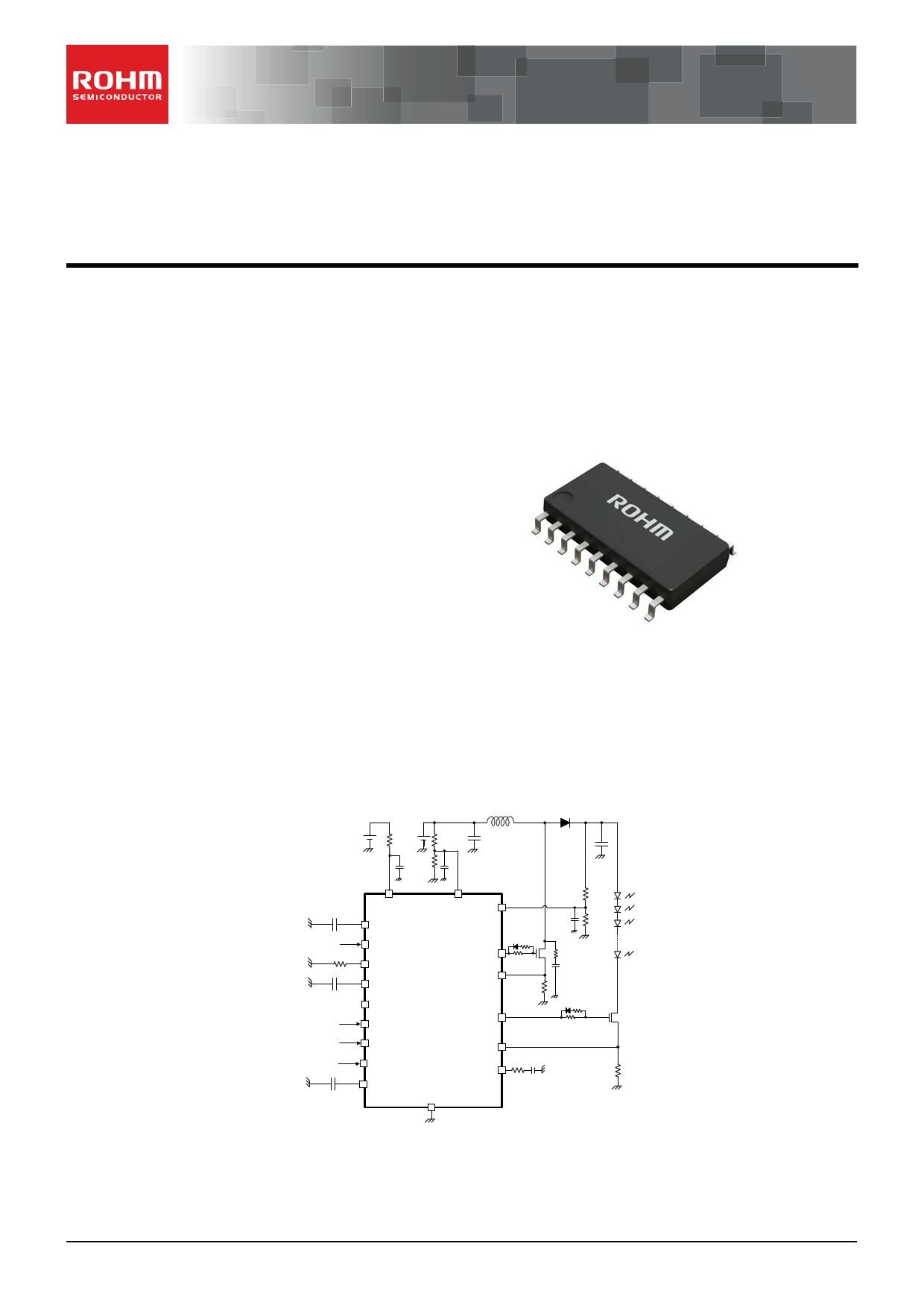
●Typical Application Circuit(s)
VCC
VIN
VCC
TC54
UVLO OVP
STB
RT
Css
SS
GATE
CS
FAILB
PWM1
DIMOUT
PWM2
ADIM_P
ADIM
GND
ISENSE
FB
Figure 2. Typical application circuit
○Product structure:Silicon monolithic integrated circuit
.www.rohm.com
© 2012 ROHM Co., Ltd. All rights reserved.
TSZ22111・14・001
○This product is not designed protection against radioactive rays
1/38
TSZ02201-0F1F0C100040-1-2
27.May 2014 Rev.003
1 page 
BD9488F
●1.3 Pin number, pin name, pin function
No. name
IN/OUT
function
1 OVP
In Over voltage protection detection pin
2 UVLO
In Under voltage lock out detection pin
3 SS
Out Slow start setting pin
4 RT
Out For DC/DC switching frequency setting pin
5 PWM1
In External PWM dimming signal input pin1
6 PWM2
In External PWM dimming signal input pin2
7 FAILB
Out Abnormality detection output pin
8 ADIM
In/Out
ADIM signal input-output pin
9 ADIM_P
In ADIM pulse signal input pin
10 GND
--
11 DIMOUT
Out Dimming signal pin for driving MOSFET
12 GATE
Out DC/DC switching output pin
13 STB
In IC On/OFF pin
14 VCC
- Power supply pin
15 ISENSE
In Current detection input pin
16 FB
17 CS
18 TC54
In/Out
In
Out
Error amplifier output pin
DC/DC output current detect pin,
OCP input pin
5.4V output pin, shutdown timer pin
rating[V]
-0.3 to 7
-0.3 to 7
-0.3 to 7
-0.3 to 7
-0.3 to 20
-0.3 to 20
-0.3 to 20
-0.3 to 20
-0.3 to 20
-0.3 to VCC
-0.3 to VCC
-0.3 to VCC
-0.3 to 20
-0.3 to 7
-0.3 to 7
-0.3 to 7
-0.3 to 7
Datasheet
www.rohm.com
© 2012 ROHM Co., Ltd. All rights reserved.
TSZ22111・15・001
5/38
TSZ02201-0F1F0C100040-1-2
27.May 2014 Rev.003
5 Page 
BD9488F
Datasheet
used for the analog dimming. In normal operation, please set the input voltage under 18.0V. For more details, please refer
to <ADIM> pin descriptions.
The input frequency of this pin assumed from 2kHz to 100kHz. Please keep in mind that the capacitor of ADIM pin is
small considering of this input frequency, the error of LED current can be cause.
○Pin10: GND
GND pin of IC.
○Pin11: DIMOUT
This is the output pin for external NMOS of dimming. The below table shows the rough output logic of each operation
state, and the output H level is VCC. Please refer to the time chart in the section 3.7 for detail explanations, because The
DIMOUT logic has the exceptional behavior. Please insert the resistance between the dimming MOS gate to improve the
over shoot of LED current, as PWM turns from low to high.
Status
Normal
Abnormal
DIMOUT output
PWM1 and PWM2
GND Level
○Pin12: GATE
This is the output terminal for driving the gate of the boost MOSFET. The high level is VCC of IC. Frequency can be set
by the resistor connected to RT. Please refer to the <RT> pin description for the frequency setting.
○Pin13: STB
ON/OFF setting terminal for IC, which can be used to perform a reset at shutdown. Please reset this pin after latch off.
Regarding of the sequence of turning on, if the input logic STB turns from low to high, the internal power supply is
activated. After the positive edge of PWM is input , BD9488 starts the boost operation.
○ The input voltage of STB pin toggles the IC state(IC ON/OFF). Please avoid the use of the intermediate level (from
0.8V to 2.2V).
Regarding of the power down sequence, while STB=L and TC54UVLO=H, in order to discharge the output voltage,
DIMOUT logic can assert high, depending on the PWM logic. This discharge behavior is separately described in the time
chart in the section 3.7.3, or in the section 3.4.2, ”how to shutdown and set TC54 capacitance”
○Pin14: VCC
Power supply pin of IC. Input range is from 9V to 18.0V.
The operation starts more than 7.5 V(TYP.) and shuts down less than 7.2 V(TYP.).
○Pin15: ISENSE
This is the input terminal for the current detection. The error amplifier
compares the lower voltage the analog dimming pin ADIM and 3.5V. The
abnormal voltage of this pin activates the protection function of LED, such as
LEDOCP, OPEN.
Vout
[LED OCP Protection Function]
More than ISENSE = 4.0V (typ.), the over current of LED (LEDOCP) will be
detected. If that states continues 130k clock of GATE pin, IC will latch off.
(Please refer to the time chart in the section 3.7.7.)
[LED OPEN Protection Function]
If OPEN state (ISENSE<0.1V) continues during 4 clocks interval of GATE
terminal, BD9488 starts to count the interval of the abnormal state. If the
abnormal condition continues by the completion of counting, BD9488 will be
latched off. (Please refer to the time chart in the section 3.7.6.)
Exceptionally the OPEN protect detection are masked in the following
conditions,
CASE1. When PWM = L. ISENSE is less than 0.1V even in normally,
because DIMOUT = L.
CASE2. In the soft-start interval. ISENSE is less than 0.1V, because of the
insufficient output voltage Vout.
DIMOUT
Error AMP
ISENSE
3.5V ADIM
FB
Figure 14. ISENSE pin circuit
○Pin16: FB
This is the output terminal of error amplifier. Monitoring the ISENSE terminal voltage, this pin outputs the error signal with
the analog dimming signal (pin ADIM) or 3.5V.
After the completion of the SS, this pin outputs high impedance as the logic “PWM1 and PWM2” asserts low. FB voltage
is hold to the external capacitance.
(For more detail on the compensation setting is described in the section " 3.6 loop compensation".)
www.rohm.com
© 2012 ROHM Co., Ltd. All rights reserved.
TSZ22111・15・001
11/38
TSZ02201-0F1F0C100040-1-2
27.May 2014 Rev.003
11 Page | ||
| Páginas | Total 30 Páginas | |
| PDF Descargar | [ Datasheet BD9488F.PDF ] | |
Hoja de datos destacado
| Número de pieza | Descripción | Fabricantes |
| BD9488F | Boost 1channel white LED driver | ROHM Semiconductor |
| Número de pieza | Descripción | Fabricantes |
| SLA6805M | High Voltage 3 phase Motor Driver IC. |
Sanken |
| SDC1742 | 12- and 14-Bit Hybrid Synchro / Resolver-to-Digital Converters. |
Analog Devices |
|
DataSheet.es es una pagina web que funciona como un repositorio de manuales o hoja de datos de muchos de los productos más populares, |
| DataSheet.es | 2020 | Privacy Policy | Contacto | Buscar |