|
|
|
PDF XC9110 Data sheet ( Hoja de datos )
| Número de pieza | XC9110 | |
| Descripción | PFM Controlled Step-Up DC/DC Converter / Controller ICs | |
| Fabricantes | Torex Semiconductor | |
| Logotipo | ||
Hay una vista previa y un enlace de descarga de XC9110 (archivo pdf) en la parte inferior de esta página. Total 30 Páginas | ||
|
No Preview Available !
XC9110/XC9111 Series
PFM Controlled Step-Up DC/DC Converter / Controller ICs
ETR0406-006a
■GENERAL DESCRIPTION
The XC9110/9111 series is a group of PFM controlled step-up DC/DC converter/controller ICs designed to generate low supply
voltage by the combination of PFM control and CMOS structure. The series is ideal for applications where a longer battery life is
needed such as in portable communication equipment. With a built-in 2.5ΩN-channel driver transistor, the XC9110A/C/E and
XC9111A/C/E types provide a step-up operation by using only a coil, a capacitor, and a diode connected externally.
The XC9110/9111B, D and F versions can be used with an external transistor for applications requiring larger currents.
Output voltage is internally programmable in a range from 1.5V to 7.0V in increments of 0.1V (accuracy: ± 2.5%).
Maximum oscillation frequency is set to 100kHz for XC9110/9111 series. (At light loads, it is set to 180kHz for the XC9111
series.) Options include products equipped with a CE pin (C and D versions) that allows the IC to be shut down thereby
reducing supply current and with separated VDD/VOUT pins (E and F versions) to separate the power supply block and the
output voltage detect block. With the XC9110 series, maximum duty cycle is set to 75% (VDD=3.3V) making it suitable for
use with large current operations. The XC9111 series automatically switches duty ratio between 56% & 75% (VDD=3.3V)
when it senses changes in load to drop output ripple voltage and can support both large and small currents. The external
transistor types (B/D/F types) can be provided for applications, which require larger currents.
■APPLICATIONS
●Mobile phones
●Various palm top equipment
●Cameras, VCRs
●Various portable equipment
■ FEATURES
Operating (Input) Range : 0.9V ~ 10.0V
Output Voltage Range
: 1.5V~7.0V in 0.1V increments
Output Accuracy
: ±2.5%
Max Oscillation Frequency : 100 kHz ±15%
180 kHz (at 56% duty of XC9111)
Built-in Switch Types
: A/C/E type
N-ch FET On-Resistance : 2.5Ω@ VDD=3.0V
External Transistor Types : B/D/F type
Lx Limit Voltage
Max Duty Cycles
: E type: more than VDD=2.0V
: A/C type: more than VOUT=2.0V
: 75% (for XC9110)
: 56%/75% two steps (for XC9111)
Low Supply Current
: 2.0μA @ VOUT=3V
Operating Ambient Temperature: -40℃~+85℃
Packages
: SOT-23 ,SOT89 (for XC9111),
SOT-25, USP-6C
Environmentally Friendly : EU RoHS Compliant, Pb Free
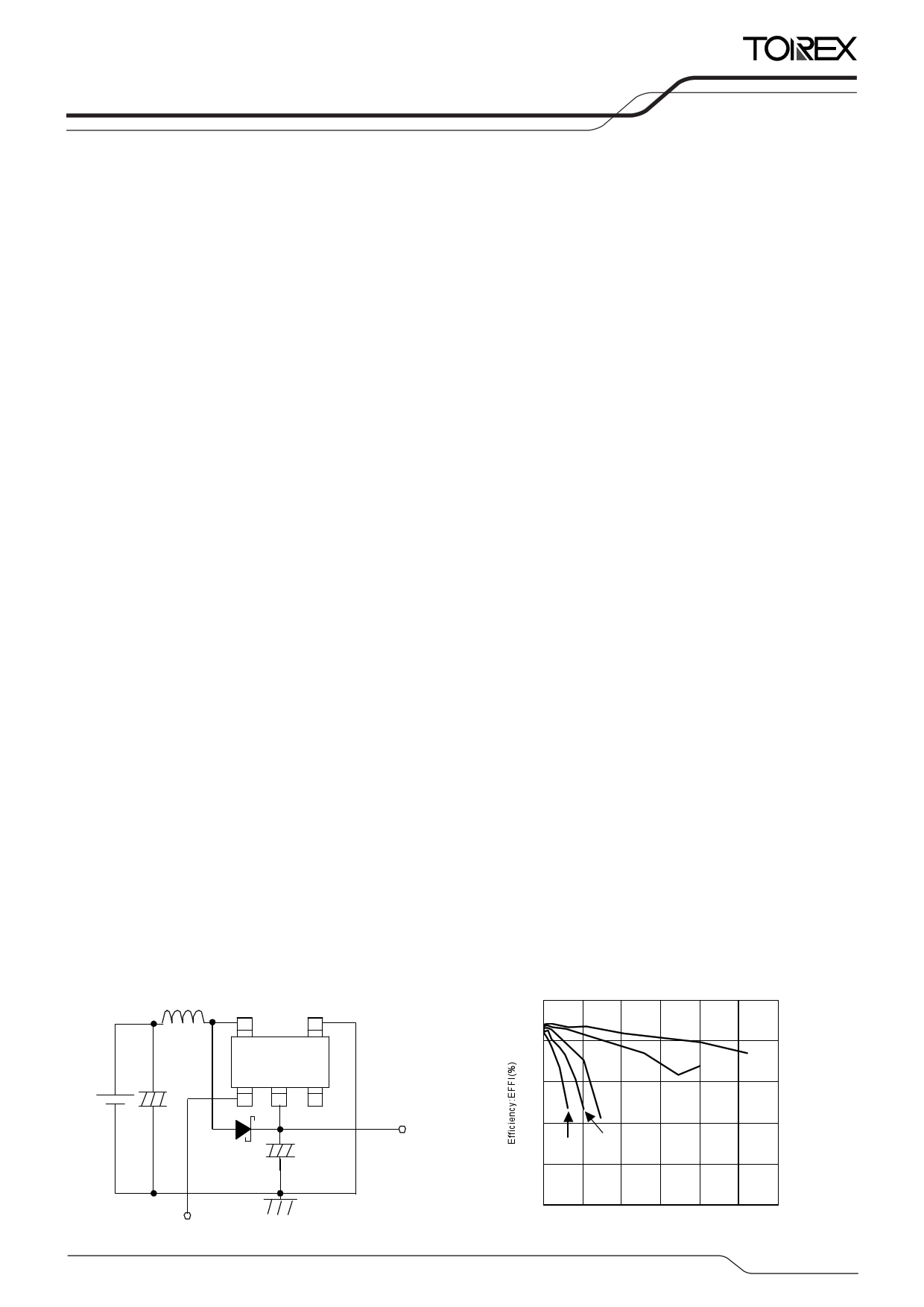
■TYPICAL APPLICATION CIRCUIT
●C type circuit
L
VIN + CIN
54
(TOP VIEW)
SOT-25
1 23
+
SD CL
(Tantalum)
GND
CE
VOUT
■TYPICAL PERFORMANCE
CHARACTERISTICS
XC9111E331MR
L=100μH(CR54), CL47μF(Tantalum)
SD: XBS104S14R-G
100
80
60
1.5V
40
1.2V
VIN=0.9V
20
3.0V
2.4V
0
0 5 0 1 00 150 2 00 250 3 00
Output Current:IOUT(mA)
1/36
1 page 
■BLOCK DIAGRAMS
●XC9110 / 9111 C and D series
XC9110/XC9111
Series
Note: The XC9110 series, Tr. Built-in type, uses the Lx pin and the XC9111 series, external Tr. Type, uses the EXT pin.
The XC9110 series' duty ratio is 75% and oscillation frequency (fOSC) is 100kHz. The duty ratio of the XC9111 series
automatically varies between 56% (oscillation frequency 180kHz) and 75% (oscillation frequency (fOSC) 100kHz). The
VLx limit function only applies to the XC9110/9111 C versions.
* The duty ratio depends on power supply. Please refer to the electrical characteristics on duty against output voltage
you use.
●XC9111 E and F series
Note: The XC9110 series, Tr. Built-in type, uses the Lx pin and the XC9111 series, external Tr. Type, uses the EXT pin.
The XC9110 / 9111 series E and F series have the VDD pin. The XC9110 series' duty ratio is 75% and
oscillation frequency (fOSC) is 100kHz. The duty ratio of the XC9111 series automatically varies between
56% (oscillation frequency 180kHz) and 75% (oscillation frequency (fOSC) 100kHz).
The VLx limit function only applies to the XC9110/9111 C versions.
* The duty ratio depends on power supply.
Please refer to the electrical characteristics on duty against output voltage you use.
5/36
5 Page 
XC9110/XC9111
Series
■ELECTRICAL CHARACTERISTICS (Continued)
XC9110Exx1MR, XC9111Exx1MR
PARAMETER
SYMBOL
CONDITIONS
MIN. TYP. MAX.
Output Voltage
VOUT
Connect to external components
×0.975 VOUT ×1.025
Output Voltage
Temperature Characteristics
Maximum Input Voltage
Operation Start Voltage
Oscillation Start Voltage
Operation Hold Voltage
Input Current
Supply Current 1 (*2)
Supply Current 2
Lx Switch ON Resistance
Lx Leak Current
Duty Ratio
Duty Ratio 2
Maximum Oscillation
Maximum Oscillation
Lx Limit Voltage (*4)
Efficiency (*5)
△VOUT
△VOUT・△topr
VIN
VST1
VST2
Connect to external components
- 40℃≦Topr≦85℃
IOUT=1mA, connect to external
components
Applied 0.8V to VOUT, Vpull=1.0V
VHLD
IOUT=1mA, connect to external
components
IIN
IDD1
IDD2
RSWON
ILxL
DTY
DTY2
MAXfOSC
MAXfOSC2
VLxLMT
IOUT=0mA (*1)
Applied (output voltage×0.95) to VOUT
Applied (output voltage+0.5V) to VOUT
Same as IDD1, VLx=0.4V (*3)
Same as IDD2, VLx=7V
Same as IDD1, measure Lx waveform
IOUT=1mA, measure Lx ON time (XC9111
only) Connect to external components
Same as IDD1
Same as IDD1 (XC9111 only)
Same as IDD1, VLx when max. oscillation
frequency is more than double.
EFFI
Connect to external components
-
10
-
-
0.7
-
-
-
-
-
E7-1(*)
48
85
153
0.7
-
±100
-
0.8
-
-
E1-1(*)
E2-1(*)
E3-1(*)
E4-1(*)
-
E7-2(*)
56
100
180
-
E8(*)
-
-
0.9
0.8
-
E1-2(*)
E2-2(*)
E3-2(*)
E4-2(*)
1
E7-3(*)
64
115
207
1.1
-
Ta = 25℃
UNIT CIRCUIT
V①
ppm/
℃
V
①
-
V①
V②
V①
μA ①
μA ②
μA ②
Ω②
μA ③
%②
%①
kHz ②
kHz ②
V②
%①
Test condition : Unless otherwise specified, connect VDD to VOUT, VIN=VOUT×0.6, IOUT=<C1(*)>, Vpull=5.0V
NOTE:
*1: TOREX SD, XBS104S14R-G is used; reverse current IR < 1μA (when reverse voltage VR = 10V is applied), in case of using
selected parts.
*2: "Supply Current 1" is the value when the IC is constantly switching. In actual operation, the oscillator periodically switches, resulting
in lower power consumption. Please refer to Input Current (IIN) under no load condition for the actual current, which is supplied
from the input power supply (VIN).
*3: Lx switch ON resistance can be calculated by (VLx x Rp) / (Vpull - VLx). * Change Vpull so that VLx will become 0.4V.
*4: The Lx limit voltage function becomes stable when VOUT of the XC9110/9111 series is over 2.0V.
*5: EFFI={[output voltage]×(output current)} / [(input voltage)×(input current)]×100
*6: When using VDD and VOUT separately, please set the voltage range of VDD from 1.5V to 10V.
The IC operates from VDD=0.8V, but output voltage and oscillation frequency will be stable when VDD=1.5V or more.
*7: Please be aware of the absolute maximum ratings of the external components.
(*): Please refer to the charts.
11/36
11 Page | ||
| Páginas | Total 30 Páginas | |
| PDF Descargar | [ Datasheet XC9110.PDF ] | |
Hoja de datos destacado
| Número de pieza | Descripción | Fabricantes |
| XC9110 | PFM Controlled Step-Up DC/DC Converter / Controller ICs | Torex Semiconductor |
| XC9111 | PFM Controlled Step-Up DC/DC Converter / Controller ICs | Torex Semiconductor |
| XC9116 | Step-Up DC/DC Converter-Backlight LED Driver | Torex Semiconductor |
| XC9119D10A | Step-Up DC/DC Converter / Ceramic Capacitor Compatible | Torex Semiconductor |
| Número de pieza | Descripción | Fabricantes |
| SLA6805M | High Voltage 3 phase Motor Driver IC. |
Sanken |
| SDC1742 | 12- and 14-Bit Hybrid Synchro / Resolver-to-Digital Converters. |
Analog Devices |
|
DataSheet.es es una pagina web que funciona como un repositorio de manuales o hoja de datos de muchos de los productos más populares, |
| DataSheet.es | 2020 | Privacy Policy | Contacto | Buscar |