|
|
|
PDF NCP1937A2DR2G Data sheet ( Hoja de datos )
| Número de pieza | NCP1937A2DR2G | |
| Descripción | Combination Power Factor Correction and Quasi- Resonant Flyback Controllers | |
| Fabricantes | ON Semiconductor | |
| Logotipo | ||
Hay una vista previa y un enlace de descarga de NCP1937A2DR2G (archivo pdf) en la parte inferior de esta página. Total 30 Páginas | ||
|
No Preview Available !
NCP1937
Combination Power Factor
Correction and Quasi-
Resonant Flyback
Controllers for Adapters
This combination IC integrates power factor correction (PFC) and
quasi−resonant flyback functionality necessary to implement a
compact and highly efficient Switched Mode Power Supply for an
adapter application.
The PFC stage exhibits near−unity power factor while operating in a
Critical Conduction Mode (CrM) with a maximum frequency clamp.
The circuit incorporates all the features necessary for building a robust
and compact PFC stage while minimizing the number of external
components.
The quasi−resonant current−mode flyback stage features a
proprietary valley−lockout circuitry, ensuring stable valley switching.
This system works down to the 4th valley and toggles to a frequency
foldback mode with a minimum frequency clamp beyond the 4th
valley to eliminate audible noise. Skip mode operation allows
excellent efficiency in light load conditions while consuming very low
standby power consumption.
Common General Features
http://onsemi.com
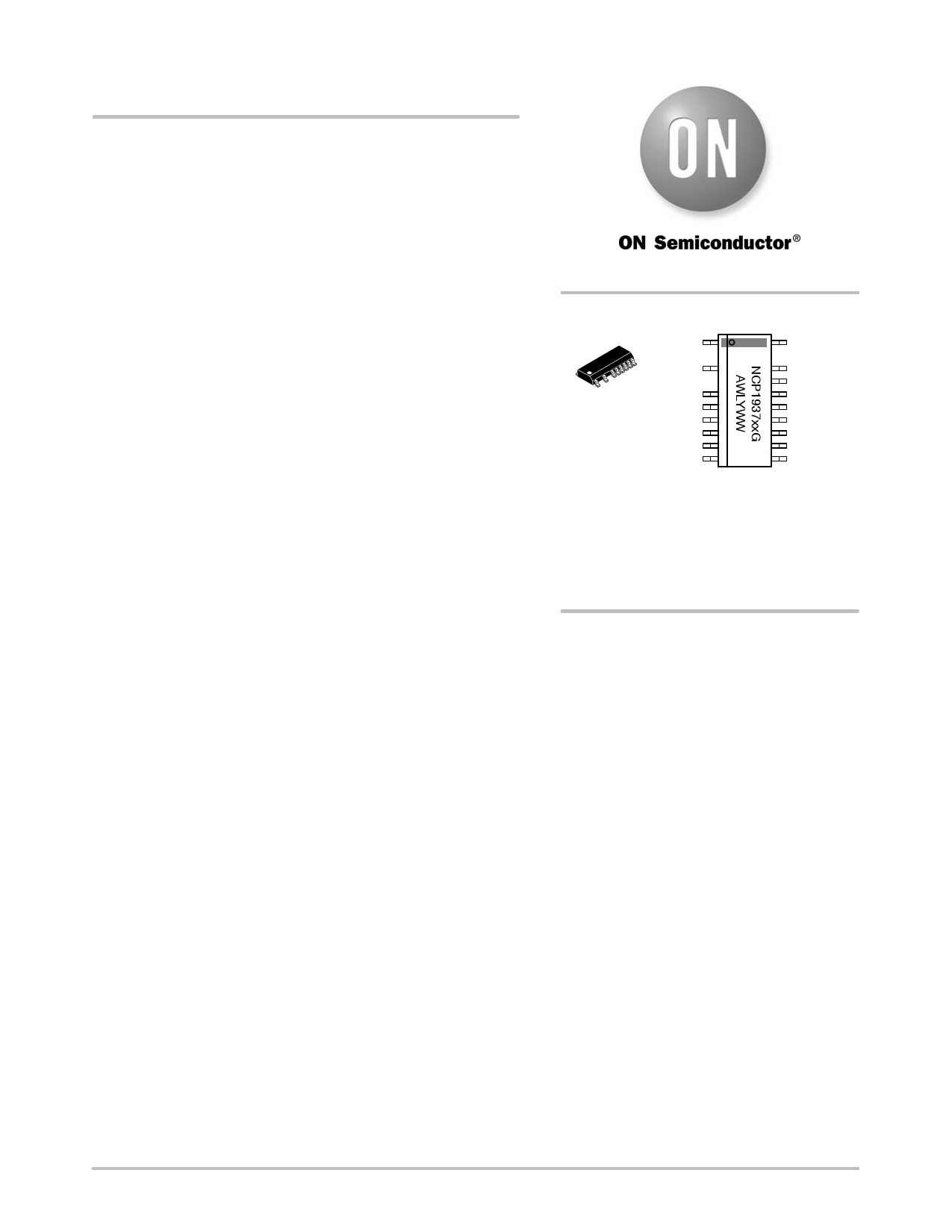
MARKING DIAGRAM
1
HV/X2
20
PFBHV
BO/X2
SOIC−20
Narrow Body
PControl
PONOFF
QCT
CASE 751BS Fault
PSTimer
QFB
PFBLV
GND
PCS/PZCD
PDRV
QDRV
QCS
VCC
QZCD
NCP1937 = Specific Device Code
xx = A1, A2, A3, B1, B2, B3, C1, C4 or C61
A = Assembly Location
WL = Wafer Lot
YY = Year
WW = Work Week
G = Pb−Free Package
• Wide VCC Range from 9 V to 30 V with Built−in Overvoltage
Protection
• High−Voltage Startup Circuit and Active Input Filter Capacitor
Discharge Circuitry for Reduced Standby Power
ORDERING INFORMATION
See detailed ordering and shipping information on page 5 of
this data sheet.
• Integrated High−Voltage Brown−Out Detector
• Integrated High−Voltage Switch Disconnects PFC Feedback Resistor
Divider to Reduce Standby Power
• Fault Input for Severe Fault Conditions, NTC
• Feed−Forward for Improved Operation across Line and
Compatible (Latch and Auto−Recovery Options)
Load
• 0.5 A / 0.8 A Source / Sink Gate Drivers
• Adjustable PFC Disable Threshold Based on Output
• Internal Temperature Shutdown
Power
• Power Savings Mode Reduces Supply Current
Consumption to 70 mA Enabling Very Low Input Power
Applications
QR Flyback Controller Features
• Valley Switching Operation with Valley−Lockout for
Noise−Free Operation
PFC Controller Features
• Critical Conduction Mode with Constant On Time
Control (Voltage Mode) and Maximum Frequency
• Frequency Foldback with Minimum Frequency Clamp
for Highest Performance in Standby Mode
• Minimum Frequency Clamp Eliminates Audible Noise
Clamp
• Accurate Overvoltage Protection
• Timer−Based Overload Protection (Latched or
Auto−Recovery options)
• Bi−Level Line−Dependent Output Voltage
• Adjustable Overpower Protection
• Fast Line / Load Transient Compensation
• Winding and Output Diode Short−Circuit Protection
• Boost Diode Short−Circuit Protection
• 4 ms Soft−Start Timer
© Semiconductor Components Industries, LLC, 2013
November, 2013 − Rev. 3
1
Publication Order Number:
NCP1937/D
1 page 
NCP1937
Table 2. NCP1937 DEVICE OPTIONS
Device
NCP1937A1DR2G
Overload
Protection
Auto−Recovery
Fault OTP
Latch
VBO(start) VBO(stop)
111 V
97 V
PFC
Disable
Time
0.5 s
PFC
Frequency
Clamp
250 kHz
Package
Shipping†
NCP1937A2DR2G Auto−Recovery
Latch
111 V
97 V
0.5 s
131 kHz
NCP1937A3DR2G Auto−Recovery
Latch
111 V
97 V
4 s 131 kHz
NCP1937B1DR2G
NCP1937B2DR2G
NCP1937B3DR2G
Auto−Recovery
Auto−Recovery
Auto−Recovery
Auto−Recovery
Auto−Recovery
Auto−Recovery
111 V
111 V
111 V
97 V
97 V
97 V
0.5 s
0.5 s
4s
250 kHz
131 kHz
131 kHz
SOIC−20 2500 / Tape
(Pb−Free) & Reel
NCP1937C1DR2G
Latch
Latch
111 V
97 V
0.5 s
250 kHz
NCP1937C4DR2G
Latch
Latch
111 V
97 V
13 s 131 kHz
NCP1937C61DR2G
Latch
Latch
101 V
87 V
4 s 131 kHz
†For information on tape and reel specifications, including part orientation and tape sizes, please refer to our Tape and Reel Packaging
Specification Brochure, BRD8011/D.
Table 3. MAXIMUM RATINGS (Notes 1 − 6)
Rating
Pin Symbol
Value
Unit
High Voltage Startup Circuit Input Voltage
1 VHV/X2
−0.3 to 700
High Voltage Startup Circuit Input Current
1 IHV/X2
20
High Voltage Brownout Detector Input Voltage
3 VBO/X2
−0.3 to 700
High Voltage Brownout Detector Input Current
3 IBO/X2
20
PFC High Voltage Feedback Input Voltage
20 VPFBHV
−0.3 to 700
PFC High Voltage Feedback Input Current
20 IPFBHV
0.5
PFC Low Voltage Feedback Input Voltage
18 VPFBLV
−0.3 to 9
PFC Low Voltage Feedback Input Current
18 IPFBLV
0.5
PFC Zero Current Detection and Current Sense Input Voltage (Note 1) 16 VPCS/PZCD
−0.3 to
VPCS/PZCD(MAX)
V
mA
V
mA
V
mA
V
mA
V
PFC Zero Current Detection and Current Sense Input Current
16 IPCS/PZCD
−2/+5
mA
PFC Control Input Voltage
5 VPControl
−0.3 to 5
V
PFC Control Input Current
5 IPControl
10
mA
Supply Input Voltage
12 VCC(MAX)
−0.3 to 30
V
Supply Input Current
12 ICC(MAX)
30
mA
Supply Input Voltage Slew Rate
12 dVCC/dt
1
V/ms
Fault Input Voltage
8
VFault
−0.3 to (VCC + 1.25)
V
Fault Input Current
8 IFault
10 mA
QR Flyback Zero Current Detection Input Voltage
11
VQZCD
−0.9 to (VCC + 1.25)
V
Stresses exceeding Maximum Ratings may damage the device. Maximum Ratings are stress ratings only. Functional operation above the
Recommended Operating Conditions is not implied. Extended exposure to stresses above the Recommended Operating Conditions may
affect device reliability.
1. VPCS/PZCD(MAX) is the maximum voltage of the pin shown in the electrical table. When the voltage on this pin exceeds 5 V, the pin sinks
a current equal to (VPCS/PZCD − 5 V) / (2 kW). A VPSC/PZCD of 7 V generates a sink current of approximately 1 mA.
2. Maximum driver voltage is limited by the driver clamp voltage, VXDRV(high), when VCC exceeds the driver clamp voltage. Otherwise, the
maximum driver voltage is VCC.
3. Maximum Ratings are those values beyond which damage to the device may occur. Exposure to these conditions or conditions beyond
those indicated may adversely affect device reliability. Functional operation under absolute maximum–rated conditions is not implied.
Functional operation should be restricted to the Recommended Operating Conditions.
4. This device contains Latch−Up protection and exceeds ± 100 mA per JEDEC Standard JESD78.
5. Low Conductivity Board. As mounted on 80 x 100 x 1.5 mm FR4 substrate with a single layer of 50 mm2 of 2 oz copper traces and heat
spreading area. As specified for a JEDEC51−1 conductivity test PCB. Test conditions were under natural convection of zero air flow.
6. Pins 1, 3, and 20 are rated to the maximum voltage of the part, or 700 V.
http://onsemi.com
5
5 Page 
NCP1937
Table 4. ELECTRICAL CHARACTERISTICS: (VCC = 12 V, VBO/X2 = 120 V, VHV/X2 = 120 V, VFault = open, VRPFBHV = 20 V,
VPFBLV = 2.4 V, VPControl = 4 V, VPCS/PZCD = 0 V, VQFB = 3 V, VPONOFF = 4 V, VQCS = 0 V, VQZCD = 0 V, VPSTimer = 0 V, RPFBHV = 200 kW,
CVCC = 100 nF , CQCT = 220 pF, CPDRV = 1 nF, CQDRV = 1 nF, for typical values TJ = 25_C, for min/max values, TJ is – 40_C to 125_C,
unless otherwise noted)
Characteristics
Conditions
Pin Symbol Min Typ Max Unit
QR FLYBACK GATE DRIVE
Rise Time (10−90%)
Fall Time (90−10%)
Driver Resistance
Current Capability
High State Voltage
Low Stage Voltage
QR FLYBACK FEEDBACK
Source
Sink
Source
Sink
VQDRV from 10 to 90%
90 to 10% of VQDRV
VQDRV = 2 V
VQDRV = 10 V
VCC = VCC(off) + 0.2 V,
RQDRV = 10 kW
VCC = 26 V,
RQDRV = 10 kW
VFault = 4 V
14
14
14
14
14
14
tQDRV(rise)
tQDRV(fall)
RQDRV(SRC)
RQDRV(SNK)
IQDRV(SRC)
IQDRV(SNK)
VQDRV(high)
VQDRV(low)
– 40 80 ns
– 20 40 ns
13 W
7
– 500 – mA
– 800 –
8– – V
10 12 14
– – 0.25 V
Internal Pull−Up Current Source
Feedback Input Open Voltage
VQFB to Internal Current Setpoint Division Ratio
QFB Pull Up Resistor
VPSTimer = 3 V;
VQFB = 0.4 V
10
IQFB
46.75 50 53.25 mA
10 VQFB(open) 4.5 5.0 5.5 V
10
KQFB
3.8 4.0 4.2
–
10 RQFB 340 400 460 kW
Valley Thresholds
Transition from 1st to 2nd valley
Transition from 2nd to 3rd valley
Transition from 3rd to 4th valley
Transition from 4th valley to VCO
Transition from VCO to 4th valley
Transition from 4th to 3rd valley
Transition from 3rd to 2nd valley
Transition from 2nd to 1st valley
Skip Threshold
Skip Hysteresis
Delay Exiting Skip Mode to 1st QDRV Pulse
Maximum On Time
QR FLYBACK TIMING CAPACITOR
VQFB decreasing
VQFB decreasing
VQFB decreasing
VQFB decreasing
VQFB increasing
VQFB increasing
VQFB increasing
VQFB increasing
VQFB decreasing
VQFB increasing
Apply 1 V step from VQSKIP
10
10
10
10
14
VH2D
VH3D
VH4D
VHVCOD
VHVCOI
VH4I
VH3I
VH2I
VQSKIP
VQSKIP(HYS)
tdelay(QSKIP)
tonQR(MAX)
1.316
1.128
0.846
0.752
1.316
1.504
1.692
1.880
0.35
25
–
26
1.400
1.200
0.900
0.800
1.400
1.600
1.800
2.000
0.40
50
–
32
1.484
1.272
0.954
0.848
1.484
1.696
1.908
2.120
0.45
75
10
38
V
V
mV
ms
ms
QCT Operating Voltage Range
VQFB = 0.5 V
7
VQCT(peak)
3.815 4.000 4.185
V
On Time Control Source Current
VQCT = 0 V
7 IQCT 18 20 22 mA
Minimum voltage on QCT Input
7 VQCT(min) – – 90 mV
Minimum Operating Frequency in VCO Mode
VQCT =10V0QmCTV(peak) +
7
fVCO(MIN)
23.5 27 30.5 kHz
http://onsemi.com
11
11 Page | ||
| Páginas | Total 30 Páginas | |
| PDF Descargar | [ Datasheet NCP1937A2DR2G.PDF ] | |
Hoja de datos destacado
| Número de pieza | Descripción | Fabricantes |
| NCP1937A2DR2G | Combination Power Factor Correction and Quasi- Resonant Flyback Controllers | ON Semiconductor |
| Número de pieza | Descripción | Fabricantes |
| SLA6805M | High Voltage 3 phase Motor Driver IC. |
Sanken |
| SDC1742 | 12- and 14-Bit Hybrid Synchro / Resolver-to-Digital Converters. |
Analog Devices |
|
DataSheet.es es una pagina web que funciona como un repositorio de manuales o hoja de datos de muchos de los productos más populares, |
| DataSheet.es | 2020 | Privacy Policy | Contacto | Buscar |