|
|
PDF TB62209FG Data sheet ( Hoja de datos )
| Número de pieza | TB62209FG | |
| Descripción | Stepping Motor Driver IC Using PWM Chopper Type | |
| Fabricantes | Toshiba Semiconductor | |
| Logotipo | ||
Hay una vista previa y un enlace de descarga de TB62209FG (archivo pdf) en la parte inferior de esta página. Total 52 Páginas | ||
|
No Preview Available !
TOSHIBA BiCD Processor IC Silicon Monolithic
TB62209FG
Stepping Motor Driver IC Using PWM Chopper Type
TB62209FG
The TB62209FG is a stepping motor driver driven by chopper
micro-step pseudo sine wave.
The TB62209FG integrates a decoder for CLK input in micro
steps as a system to facilitate driving a two-phase stepping motor
using micro-step pseudo sine waves. Micro-step pseudo sine
waves are optimal for driving stepping motors with low-torque
ripples and at low oscillation. Thus, the TB62209FG can easily
drive stepping motors with low-torque ripples and at high
efficiency.
Also, TB62209FG consists of output steps by DMOS (Power
MOS FET), and that makes it possible to control the output
Weight: 0.79 g (typ.)
power dissipation much lower than ordinary IC with bipolar
transistor output.
The IC supports Mixed Decay mode for switching the attenuation ratio at chopping. The switching time for the
attenuation ratio can be switched in four stages according to the load.
Features
• Bipolar stepping motor can be controlled by a single driver IC
• Monolithic BiCD IC
• Low ON-resistance of Ron = 0.5 Ω (Tj = 25°C @1.0 A: typ.)
• Built-in decoder and 4-bit DA converters for micro steps
• Built-in ISD, TSD, VDD &VM power monitor (reset) circuit for protection
• Built-in charge pump circuit (two external capacitors)
• 36-pin power flat package (HSOP36-P-450-0.65)
• Output voltage: 40 V max
• Output current: 1.8 A/phase max
• 2-phase, 1-2 (type 2) phase, W1-2 phase, 2W1-2 phase, 4W1-2 phase, or motor lock mode can be
selected.
• Built-in Mixed Decay mode enables specification of four-stage attenuation ratio.
• Chopping frequency can be set by external resistors and capacitors.
High-speed chopping possible at 100 kHz or higher.
Note: When using the IC, pay attention to thermal conditions.
This device is easily damaged by high static voltage, please handle with care.
This product is RoHS compatible.
1 2010-07-02
1 page 
TB62209FG
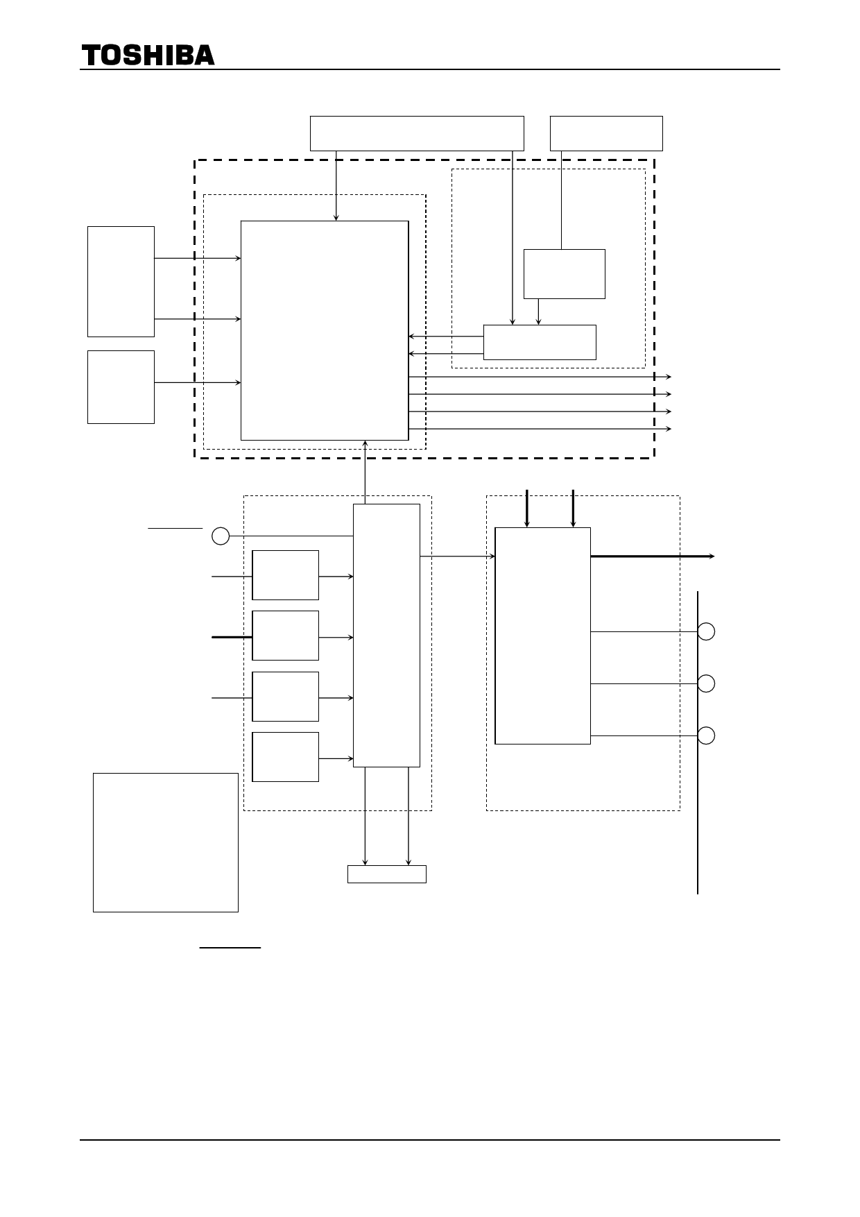
4. Output control circuit, current feedback circuit and current setting circuit
Micro-step current setting
decoder circuit
Chopping
reference circuit
Current
feedback
circuit
Current
setting
circuit
Output control circuit
PHASE
NF set current
reached signal
RNF set current
monitor signal
Mixed
Decay
timing
Output stop
signal
Charge Start
U1
U2
L1
Output control circuit
L2
DECAY
MODE
Mixed
Decay
timing
circuit
CR counter
CR Selector
Output circuit
STANDBY
Output pin
VM
VDD
ISD
circuit
VMR
circuit
VDDR
circuit
Output RESET signal
VDD
VM
Power supply for
upper drive output
Internal
stop
signal
select
circuit
Charge
pump
halt
signal
Charge
pump
circuit
VH
VDDR: VDD power on
Reset
VMR: VM power on Reset
ISD: Current shutdown
circuit
TSD: Thermal shutdown
circuit
TSD
circuit
Protection
circuit
Micro-step current
setup latch
clear signal
LOGIC
Charge pump
circuit
Mixed Decay
timing table clear
signal
Output
circuit
Cop A
Cop B
Cop C
Note: The STANDBY pins are pulled down in the IC by 100-kΩ resistor.
When not using the pin, connect it to GND. Otherwise, malfunction may occur.
5 2010-07-02
5 Page 
Pin Description 3
TB62209FG
Pin Number Pin Name
25 NC
26 OUT A
27 PGND
FIN FIN
28 PGND
29 OUT B
30 NC
31 DATA MODE
32 RESET
33 OUT B
34 ENABLE
35 CLK
36 CR
Function
Remarks
Not connected
Not wired
Channel A output pin
―
Power ground pin
Logic ground pin
Connect all power ground pins and VSS to GND.
The pin functions as a heat sink. Design pattern
taking heat into consideration.
Power ground pin
Connect all power ground pins to GND.
Channel B output pin
―
Not connected
Not wired
H: Controls external PWM.
L: CLK-IN mode
Clock input and PWM
We recommend this pin normally be used as
CLK-IN mode pin (Low).
In PWM mode, functions such as constant
current control do not operate. Fix DATA MODE
at the L level.
Forcibly initializes electrical angle.
Initializes electrical angle.
At this time we recommend ENABLE pin be set
to Low to prevent miss operation.
H: Resets electrical angle.
L: Normal operation
Channel B output pin
⎯
Output enable pin
Forcibly turns all output transistors off.
Inputs CLK for determining number of motor
rotations.
Electrical angle is incremented by one for each
CLK input.
CLK is reflected at rising edge.
Chopping reference frequency reference pin (for
setting chopping frequency)
Determines chopping frequency.
11 2010-07-02
11 Page | ||
| Páginas | Total 52 Páginas | |
| PDF Descargar | [ Datasheet TB62209FG.PDF ] | |
Hoja de datos destacado
| Número de pieza | Descripción | Fabricantes |
| TB62209F | Stepping Motor Driver IC Using PWM Chopper Type | Toshiba |
| TB62209FG | Stepping Motor Driver IC Using PWM Chopper Type | Toshiba Semiconductor |
| Número de pieza | Descripción | Fabricantes |
| SLA6805M | High Voltage 3 phase Motor Driver IC. |
Sanken |
| SDC1742 | 12- and 14-Bit Hybrid Synchro / Resolver-to-Digital Converters. |
Analog Devices |
|
DataSheet.es es una pagina web que funciona como un repositorio de manuales o hoja de datos de muchos de los productos más populares, |
| DataSheet.es | 2020 | Privacy Policy | Contacto | Buscar |
