|
|
|
PDF MJE13005A Data sheet ( Hoja de datos )
| Número de pieza | MJE13005A | |
| Descripción | Switchmode Series NPN Silicon Power Transistors | |
| Fabricantes | nELL | |
| Logotipo | ||
Hay una vista previa y un enlace de descarga de MJE13005A (archivo pdf) en la parte inferior de esta página. Total 6 Páginas | ||
|
No Preview Available !
SEMICONDUCTOR
MJE13005A(NPN) RRooHHSS
Nell High Power Products
Switchmode Series NPN Silicon Power Transistors
(4A / 400V / 75W)
FEATURES
VCEO(SUS) ≥ 400V @ lC = 10 mA, lB = 0
VCE(sat) = 1.0V (Max.) @ lC = 4 A, lB = 1 A
Switching time - tf = 0.9 µs (Max.) @ lC = 2 A
700V blocking capability
DESCRIPTION
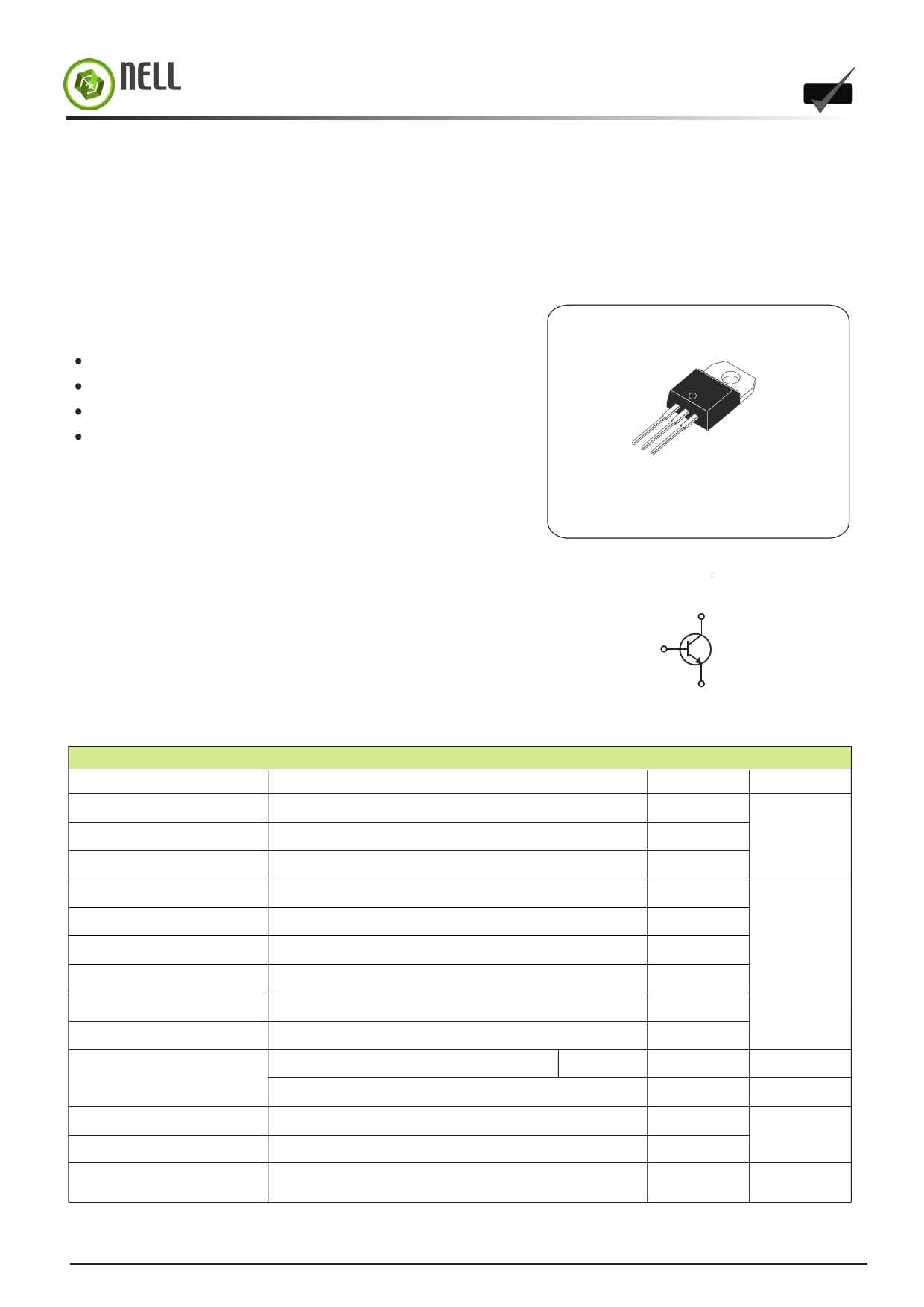
123
TO-220AB
(MJE13005A)
These devices are designed for high-voltage,
high-speed power switching inductive circuits
where fall time is critical. They are particularly
suited for 115 and 220V SWITCHMODE
applications such as switching regulators,
inverters, motor controls, solenoid/relay drivers
and deflection circuits.
INTERNAL SCHEMATIC DIAGRAM
C (TAB)
(1)
B
(2)
E
(NPN)
ABSOLUTE MAXIMUM RATINGS (TC = 25°C unless otherwise specified)
SYMBOL
PARAMETER
VCEV
Collector to base voltage (VBE = 0)
VCEO
Collector to emitter voltage (IB = 0)
VEBO
Emitter to base voltage
IC Collector current - continuous
ICM Peak collector current (Note 1)
IB Base current - continuous
IBM Peak base current (Note 1)
IE Emitter current - continuous
IEM Peak emitter current (Note 1)
Total power dissipation
PD
Derate above 25ºC
TC= 25°C
Tj Junction temperature
Tstg Storage temperature
TL
Maximum lead temperature for soldering purposes:
1/16” from case for ≤ 10 seconds
Note: 1. Pulse test : Pulse width = 5ms, duty cycle ≤ 10%
VALUE
700
400
9
4
8
2
4
6
12
75
0.6
150
-65 to 150
265
UNIT
V
A
W
W/ºC
ºC
ºC
www.nellsemi.com
Page 1 of 6
http://www.Datasheet4U.com
1 page 
SEMICONDUCTOR
MJE13005A(NPN) RRooHHSS
Nell High Power Products
Fig.10 Typical thermal response【Zth(j-c)(t)】
1
0.7
D = 0.5
0.5
0.3
0.2 0.2
0.1
0.07
0.05
0.03
0.02
0.1
0.05
0.02
0.01
SINGLE PULSE
0.01
0.01 0.02 0.05 0.1 0.2
0.5 1
P(pk)
Zth(j-c)(t) = r(t) Rth(j-c)
Rth(j-c)= 1.67°C/W MAX
D CURVES APPLY FOR POWER
PULSE TRAIN SHOWN
READ TIME AT t1
TJ(PK) - TC = P(pK) Zth(j-c)(t)
t1
t2
DUTY CYCLE, D = t1/t2
2 5 10 20 50
100 200 500 1K
time,t (ms)
Fig.11 Forward bias safe operating area
(FBSOA)
10
5
2
1
0.5
0.2
0.1
0.05
0.02
0.01
5
5 ms
dc
Bonding wire limited
Thermally limited
TC = 25°C (single pulse)
Second breardown limited
Tj = 150°C
7 10
20 30 50 70 100
500 µs
1 ms
MJE13005A
200 300 500
Collector-Emitter voltage, VCE (V)
Fig.12 Reverse bias switching safe operating area
(RBSOA)
4
TC ≤ 100°C
lB1 = 2.0A
3
2
VB1(off) = 9V
1
MJE13005A
5V
3V
0 1.5V
0 100 200 300 400 500 600 700 800
Collector-Emitter voltage, VCE (V)
FORWARD BIAS
There are two limitations on the power handling ability
of a transistor:average junction temperature and second
breakdown. Safe operating area curves indicate lC - VCE
limits of the transistor that must be observed for reliable
operation; i.e., the transistor must not be subjected to
greater dissipation than the curves indicate.
The data of Fig.11 is based on TC = 25°C ; TJ(pk) is
variable depending on power level. Second breakdown
pulse limits are valid for duty cycles to 10% but must be
derated when TC ≥ 25°C. Second breakdown limitations
do not derate the same as thermal limitations. Allowable
current at the voltages shown on Fig.11 may be found at
any case temperature by using the appropriate curve on
Fig.13.
TJ(pk) may be calculated from the data in Fig.10. At high
case temperatures, thermal limitations will reduce the
power that can be handled to values less than the
limitations mposed by second breakdown.
REVERSE BLAS
For inductive loads, high voltage and high current
must be sustained simultaneously during turn-off, in
most cases, with the base to emitter junction reverse
biased. Under these conditions the collector voltage
must be held to a safe level at or below a specific value
of collector current. This can be accomplished by several
means such as active clamping, RC snubbing, load line
shaping, etc. The safe level for these devices is specified
as Reverse Bias Safe Operating Area and repesents the
voltage-current conditions during reverse biased turn-off.
This rating is verified under clamped conditions so that the
device is never subjected to an avalanche mode. Fig.12
gives the complete RBSOA characteristics.
www.nellsemi.com
Page 5 of 6
5 Page | ||
| Páginas | Total 6 Páginas | |
| PDF Descargar | [ Datasheet MJE13005A.PDF ] | |
Hoja de datos destacado
| Número de pieza | Descripción | Fabricantes |
| MJE13005 | TRANSISTORS | SI Semiconductors |
| MJE13005 | 4 AMPERE NPN SILICON POWER TRANSISTOR 400 VOLTS 75 WATTS | Motorola Semiconductors |
| MJE13005 | NPN SILICON POWER TRANSISTOR | ON |
| MJE13005 | NPN SILICON TRANSISTOR(ELECTRONIC TRANSFORMERS / POWER SWICHING CIRCUIT) | Wing Shing Computer Components |
| Número de pieza | Descripción | Fabricantes |
| SLA6805M | High Voltage 3 phase Motor Driver IC. |
Sanken |
| SDC1742 | 12- and 14-Bit Hybrid Synchro / Resolver-to-Digital Converters. |
Analog Devices |
|
DataSheet.es es una pagina web que funciona como un repositorio de manuales o hoja de datos de muchos de los productos más populares, |
| DataSheet.es | 2020 | Privacy Policy | Contacto | Buscar |