|
|
|
PDF 24LC32 Data sheet ( Hoja de datos )
| Número de pieza | 24LC32 | |
| Descripción | 32KI2CSerialEEPROMinISOMicromodule | |
| Fabricantes | MicrochipTechnology | |
| Logotipo | ||
Hay una vista previa y un enlace de descarga de 24LC32 (archivo pdf) en la parte inferior de esta página. Total 16 Páginas | ||
|
No Preview Available !
M 24LC32A MODULE
32K I2C™ Serial EEPROM in ISO Micromodule
FEATURES
• ISO 7816 compliant contact locations
• Single supply with operation down to 2.5V
- Maximum write current 3 mA at 6.0V
- Maximum read current 150 µA at 6.0V
- Standby current 1 µA max at 2.5V
• Two wire serial interface bus, I2C™ compatible
• 100 kHz (2.5V) and 400 kHz (5V) compatibility
• Self-timed ERASE and WRITE cycles
• Power on/off data protection circuitry
• 1,000,000 ERASE/WRITE cycles guaranteed
• 32 byte page or byte write modes available
• Schmitt trigger inputs for noise suppression
• Output slope control to eliminate ground bounce
• 2 ms typical write cycle time, byte or page
• Electrostatic discharge protection > 4000V
• Data retention > 200 years
• 8-pin PDIP and SOIC packages
• Temperature ranges:
- Commercial:
0˚C to +70˚C
DESCRIPTION
The Microchip Technology Inc. 24LC32A is a 4K x 8
(32K bit) Serial Electrically Erasable PROM in an ISO
micromodule for use in smart card applications. The
device has a page-write capability of up to 32 bytes.
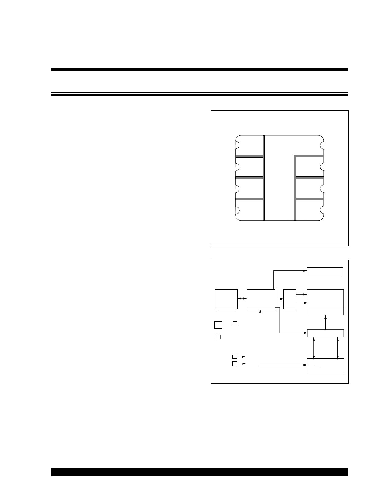
ISO MODULE LAYOUT
VDD
VSS
SCL SDA
BLOCK DIAGRAM
HV GENERATOR
I/O
CONTROL
LOGIC
MEMORY
CONTROL
LOGIC
I/O
SCL
SDA
VCC
VSS
XDEC
EEPROM
ARRAY
PAGE LATCHES
YDEC
SENSE AMP
R/W CONTROL
I2C is a trademark of Philips Corporation.
© 1997 Microchip Technology Inc.
DS21225A-page 1
1 page 
24LC32A MODULE
4.0 BUS CHARACTERISTICS
The following bus protocol has been defined:
• Data transfer may be initiated only when the bus
is not busy.
• During data transfer, the data line must remain
stable whenever the clock line is HIGH. Changes
in the data line while the clock line is HIGH will be
interpreted as a START or STOP condition.
Accordingly, the following bus conditions have been
defined (See Figure 4-1).
4.1 Bus not Busy (A)
Both data and clock lines remain HIGH.
4.2 Start Data Transfer (B)
A HIGH to LOW transition of the SDA line while the
clock (SCL) is HIGH determines a START condition.
All commands must be preceded by a START condi-
tion.
4.3 Stop Data Transfer (C)
A LOW to HIGH transition of the SDA line while the
clock (SCL) is HIGH determines a STOP condition. All
operations must be ended with a STOP condition.
4.4 Data Valid (D)
The state of the data line represents valid data when,
after a START condition, the data line is stable for the
duration of the HIGH period of the clock signal.
The data on the line must be changed during the LOW
period of the clock signal. There is one clock pulse per
bit of data.
Each data transfer is initiated with a START condition
and terminated with a STOP condition. The number of
the data bytes transferred between the START and
STOP conditions is determined by the master device.
4.5 Acknowledge
Each receiving device, when addressed, is obliged to
generate an acknowledge signal after the reception of
each byte. The master device must generate an extra
clock pulse which is associated with this acknowledge
bit.
Note:
The 24LC32A does not generate any
acknowledge bits if an internal program-
ming cycle is in progress.
A device that acknowledges must pull down the SDA
line during the acknowledge clock pulse in such a way
that the SDA line is stable LOW during the HIGH period
of the acknowledge related clock pulse. Of course,
setup and hold times must be taken into account. Dur-
ing reads, a master must signal an end of data to the
slave by NOT generating an acknowledge bit on the
last byte that has been clocked out of the slave. In this
case, the slave (24LC32A) will leave the data line HIGH
to enable the master to generate the STOP condition.
(See Figure 4-2)
FIGURE 4-1: DATA TRANSFER SEQUENCE ON THE SERIAL BUS
SCL
(A)
(B)
(D)
(D)
(C) (A)
SDA
START
CONDITION
DATA OR
DATA
ACKNOWLEDGE ALLOWED
VALID
TO CHANGE
FIGURE 4-2: ACKNOWLEDGE TIMING
Acknowledge
Bit
STOP
CONDITION
SCL 1 2 3 4 5 6 7 8 9 1 2 3
SDA
Data from transmitter
Transmitter must release the SDA line at this point allowing the Receiver
to pull the SDA line low to acknowledge the previous eight bits of data.
Data from transmitter
Receiver must release the SDA line at this point
so the Transmitter can continue sending data.
© 1997 Microchip Technology Inc.
DS21225A-page 5
5 Page 
FIGURE 9-2: MODULE DIMENSIONS
24LC32A MODULE
© 1997 Microchip Technology Inc.
DS21225A-page 11
11 Page | ||
| Páginas | Total 16 Páginas | |
| PDF Descargar | [ Datasheet 24LC32.PDF ] | |
Hoja de datos destacado
| Número de pieza | Descripción | Fabricantes |
| 24LC32 | 32KI2CSerialEEPROMinISOMicromodule | MicrochipTechnology |
| 24LC320-IP | 32K2.5VSPIBusSerialEEPROM | MicrochipTechnology |
| 24LC320-ISN | 32K2.5VSPIBusSerialEEPROM | MicrochipTechnology |
| 24LC320-IST | 32K2.5VSPIBusSerialEEPROM | MicrochipTechnology |
| Número de pieza | Descripción | Fabricantes |
| SLA6805M | High Voltage 3 phase Motor Driver IC. |
Sanken |
| SDC1742 | 12- and 14-Bit Hybrid Synchro / Resolver-to-Digital Converters. |
Analog Devices |
|
DataSheet.es es una pagina web que funciona como un repositorio de manuales o hoja de datos de muchos de los productos más populares, |
| DataSheet.es | 2020 | Privacy Policy | Contacto | Buscar |