|
|
PDF UT3232 Data sheet ( Hoja de datos )
| Número de pieza | UT3232 | |
| Descripción | 3.0V TO 5.5V LOW POWER MULTICHANNEL RS-232 LINE TRANSCEIVERS USING | |
| Fabricantes | UNISONIC TECHNOLOGIES | |
| Logotipo |  |
|
Hay una vista previa y un enlace de descarga de UT3232 (archivo pdf) en la parte inferior de esta página. Total 7 Páginas | ||
|
No Preview Available !
UNISONIC TECHNOLOGIES CO., LTD
UT3232
Preliminary
CMOS IC
3.0V TO 5.5V LOW POWER
MULTICHANNEL RS-232 LINE
TRANSCEIVERS USING FOR
0.1μF EXTERNAL CAPACITORS
DESCRIPTION
The UTC UT3232 have two receivers and two drivers, and a dua l
charge-pump circuit. T he devic e meets the req uirements o f
TIA/EIA-232-F and p rovides the el ectrical i nterface be tween a n
asynchronous communication controller and the serial-port connector.
The charge p ump and fo ur small external capacitors allow operation
from a single 3. 0V to 5. 5V su pply. T he device operates at data
signaling rates up to 250kbit/s and a maximum of 35V/μs driver output
slew rate.
SOP-16
TSSOP-16
FEATURES
* Exceeds ±8KV ESD Protection(HBM) for RS-232 I/O Pins
* Meets the Requirements of TIA/EIA-232-F and ITU V.28 Standards
* Operates With 3.0V to 5.5V VCC Supply
* Operates Up To 250kbit/s Data Rate
* Two Drivers and Two Receivers
* External Capacitors 4×0.1μF
* Accepts 5.0V Logic Input With 3.3V Supply
ORDERING INFORMATION
Ordering Number
Lead Free
Halogen Free
UT3232L-P16-T UT
3232G-P16-T
UT3232L-P16-R UT
3232G-P16-R
Package Packing
SOP-16
SOP-16
Tube
Tape Reel
www.unisonic.com.tw
Copyright © 2014 Unisonic Technologies Co., Ltd
1 of 7
QW-R502-A68.b
http://www.Datasheet4U.com
1 page 
UT3232
Preliminary
CMOS IC
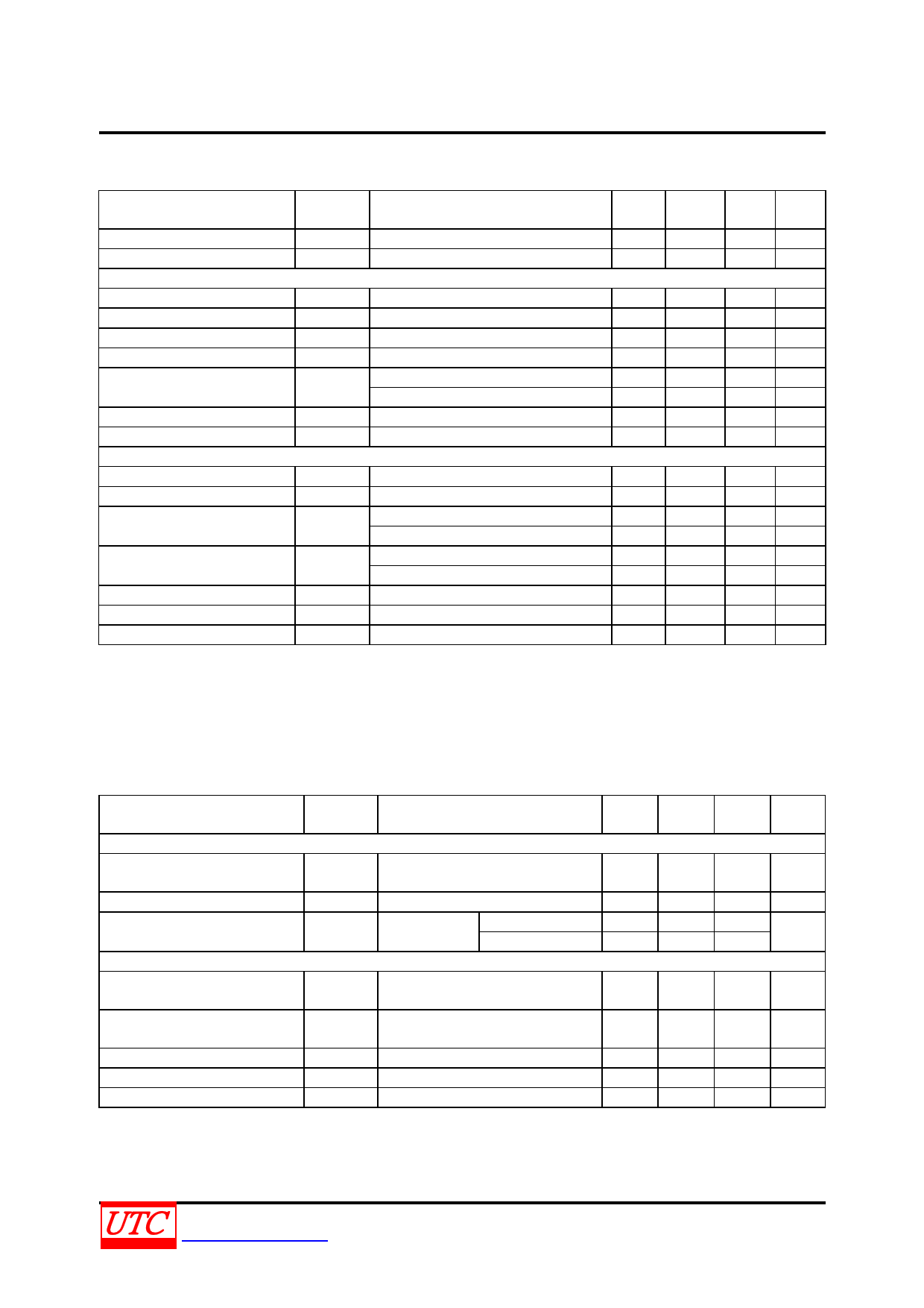
ELECTRICAL CHARACTE RISTICS [(over recommende d ran ges of suppl y voltage and operating
free-air temperature (unless otherwise noted) (see Note 3 & Table 1)]
PARAMETER
SYMBOL
TEST CONDITIONS
MIN
TYP
(Note 1)
MAX
UNIT
Input Leakage Current
Supply Current
IIN DIN
ICC No
load
±0.01 ±1 μA
0.3 1.0 mA
DRIVER SECTION
High-Level Output Voltage
VOH DOUT at RL=3kΩ to GND, DIN=GND +5.0 +5.4
V
Low-Level Output Voltage
VOL DOUT at RL=3kΩ to GND, DIN=VCC -5.0
-5.4
V
High-Level Input Current
IOH VI=VCC
±0.01 ±1 μA
Low-Level Input Current
Short-Circuit Output Current
(Note 2)
Output Resistance
IOL VI at GND
IOS
VCC=3.6V, VOUT=0V
VCC=5.5V, VOUT=0V
rO VCC, V+ and V- =0V, VOUT=±2.0V 300
±0.01 ±1 μA
±35 ±60 mA
±35 ±60 mA
10M Ω
Output Leakage Current
IOFF VCC=3.0V~5.5V, VOUT=±12V
±25 μA
RECEIVER SECTION
High-Level Output Voltage
Low-Level Output Voltage
VOH IOH=-1.0mA
VOL IOL=1.6mA
VCC-0.6V V CC- 0.1V
V
0.4
V
Positive-Going Input Threshold
Voltage
VIT+
VCC=3.3V
VCC=5.0V
1.5 2.4 V
1.8 2.4 V
Negative-Going Input
Threshold Voltage
VIT-
VCC=3.3V 0.6
VCC=5.0V 0.8
1.2 V
1.5 V
Input Hysteresis
Output Leakage Current
VHYS
IOFF
VIT+~VIT-
0.3
±0.05
±10
V
µA
Input Resistance
RI VI=±3.0V~±25V
3 5 7 kΩ
Notes: 1. All typical values are at VCC=3.3V or VCC=5.0V, and TA=25°C.
2. Short-circuit durations should be controlled to prevent exceeding the device absolute power-dissipation
ratings, and not more than one output should be shorted at a time.
3. Test conditions are C1~C4=0.1μF at VCC=3.3V±0.3V; C1=0.047μF, C2~C4=0.33μF at VCC=5.0V±0.5V.
4. Pulse skew is defined as |tPLH−tPHL| of each channel of the same device.
SWITCHING CH ARACTERISTICS [over reco mmended ra nges of s upply voltag e a nd operating
free-air temperature (unless otherwise noted) (see Note 3 and Table 1)]
PARAMETER
SYMBOL
TEST CONDITIONS
MIN
TYP
(Note 1)
MAX UNIT
DRIVER SECTION
Maximum Data Rate
CL=1000pF, RL=3kΩ, One Driver
Switching
150 250
Kbit/s
Pulse Skew (Note 4)
tSK(p) CL=220pF~2500pF, RL =3kΩ~7kΩ
300
ns
Slew Rate, Transition Region
SR(tr)
RL =3kΩ~7kΩ, CL=220pF~1000pF
VCC=3.3V
CL=220pF~2500pF
5
3
35
35
V/μs
RECEIVER SECTION
Propagation Delay Time, Low-
to High-Level Output
tPLH CL=150pF
300 ns
Propagation Delay Time, High-
to Low-Level Output
tPHL CL=150pF
300 ns
Output Enable Time
tEN CL=150pF, RL=3kΩ
200 ns
Output Disable Time
tDIS CL=150pF, RL=3kΩ
200 ns
Pulse Skew (Note 4)
tSK(P) |t PLH−tPHL|
300 ns
Notes: 1. All typical values are at VCC=3.3V or VCC=5.0V, and TA=25°C.
2. Short-circuit durations should be controlled to prevent exceeding the device absolute power-dissipation
ratings, and not more than one output should be shorted at a time.
3. Test conditions are C1~C4=0.1μF at VCC=3.3V±0.3V; C1=0.047μF, C2~C4=0.33μF at VCC=5.0V±0.5V.
4. Pulse skew is defined as |tPLH−tPHL| of each channel of the same device.
UNISONIC TECHNOLOGIES CO., LTD
www.unisonic.com.tw
5 of 7
QW-R502-A68.b
5 Page | ||
| Páginas | Total 7 Páginas | |
| PDF Descargar | [ Datasheet UT3232.PDF ] | |
Hoja de datos destacado
| Número de pieza | Descripción | Fabricantes |
| UT3232 | 3.0V TO 5.5V LOW POWER MULTICHANNEL RS-232 LINE TRANSCEIVERS USING | UNISONIC TECHNOLOGIES |
| Número de pieza | Descripción | Fabricantes |
| SLA6805M | High Voltage 3 phase Motor Driver IC. |
Sanken |
| SDC1742 | 12- and 14-Bit Hybrid Synchro / Resolver-to-Digital Converters. |
Analog Devices |
|
DataSheet.es es una pagina web que funciona como un repositorio de manuales o hoja de datos de muchos de los productos más populares, |
| DataSheet.es | 2020 | Privacy Policy | Contacto | Buscar |
